


| Technical Name | GaN Based High-frequency High-efficiency Converter | ||
|---|---|---|---|
| Project Operator | National Central University | ||
| Project Host | 辛裕明 | ||
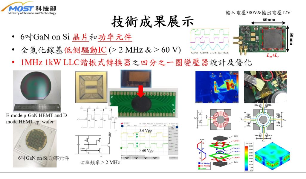
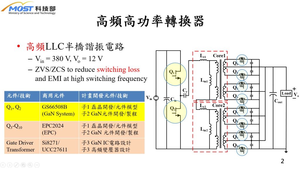
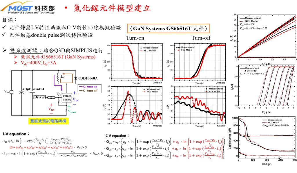
| Summary | A high power converter application built with GaN HEMT was presented. The technical aspects are developed from 6-inch wafers to converter applications, covering the optimization of 6-inch GaN epitaxial layers. The processdevice model of the 6-inch GaN E/D-mode component was established. Low-side GaN HEMT logic gates ( 2MHz) for integrated circuit were designed. Finally, The high-frequency LLC resonant converter is completed. |
||
| Scientific Breakthrough | The high power converter system constructed with wide bandgap (GaN HEMT) is currently tested to 1 MHz/1000 W with a power density of 38 W/cm3a conversion efficiency of 97. The technology starts from the 6-inch wafer to the system application including the optimization of 6-inch GaN epitaxy. E/D-mode HEMT fabrication,Low-side GaN HEMT logic gate ( 2MHz) for integrated circuit design. |
||
| Industrial Applicability | Industrial applicability can be applied by the most upstream epitaxial technology, the midstream process technologycomponent model,the final converter/converter circuit (transformer). It is in line with Taiwan's semiconductor industry's additional GaN options in Silicon. |
||
| Keyword | GaN Converter HEMT epitaxial E-mode HEMT D-mode HEMT Device Modeling Diode Gate Driver GaN-based IC | ||
- Cain@ce.ncu.edu.tw
other people also saw