

| Technical Name | Quantum Sensing with Fluorescent Nanodiamonds for Advanced Semiconductor Applications | ||
|---|---|---|---|
| Project Operator | Institute of Atomic and Molecular Sciences, Academia Sinica | ||
| Project Host | 張煥正 | ||
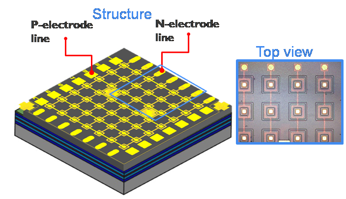
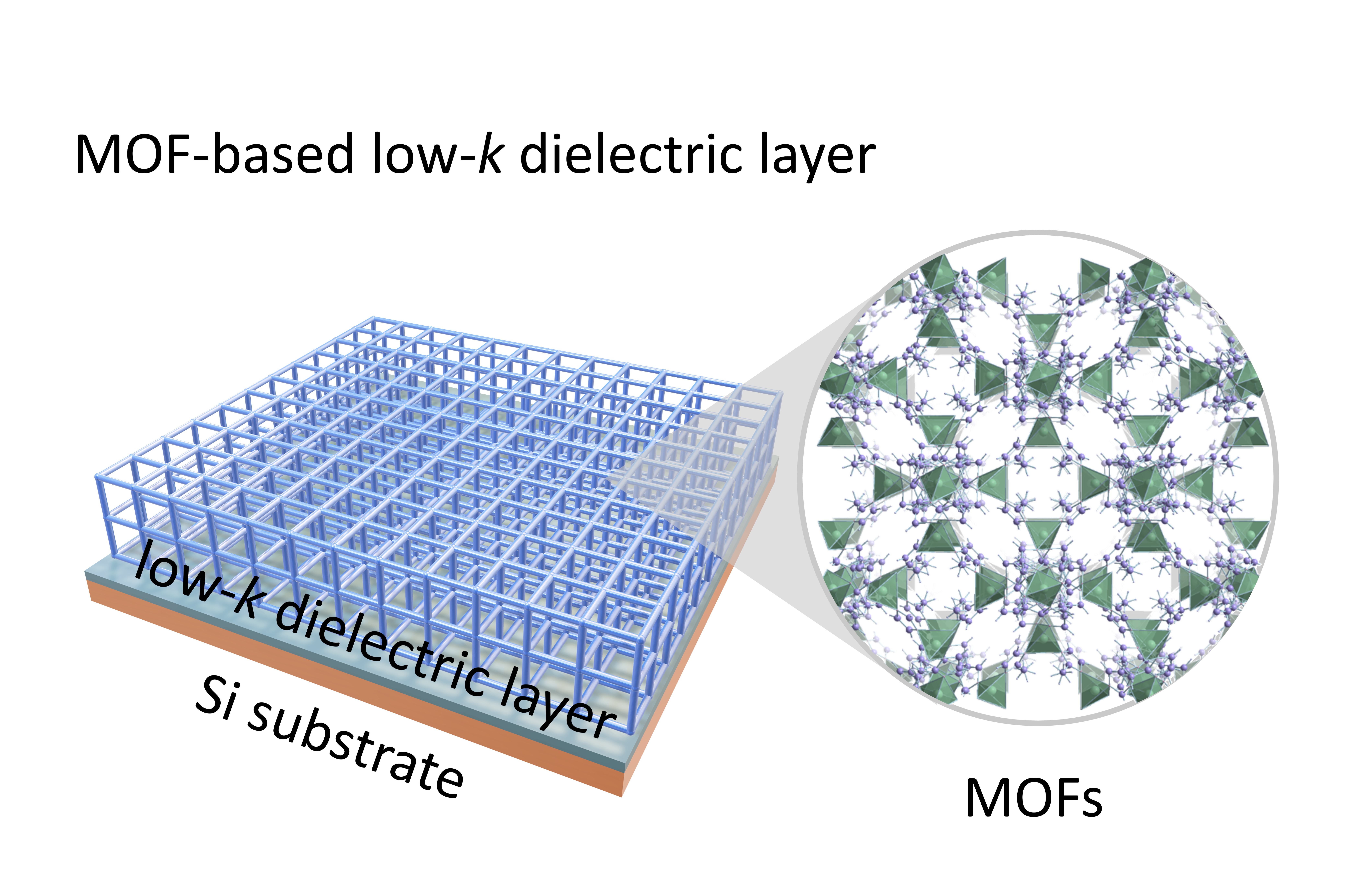
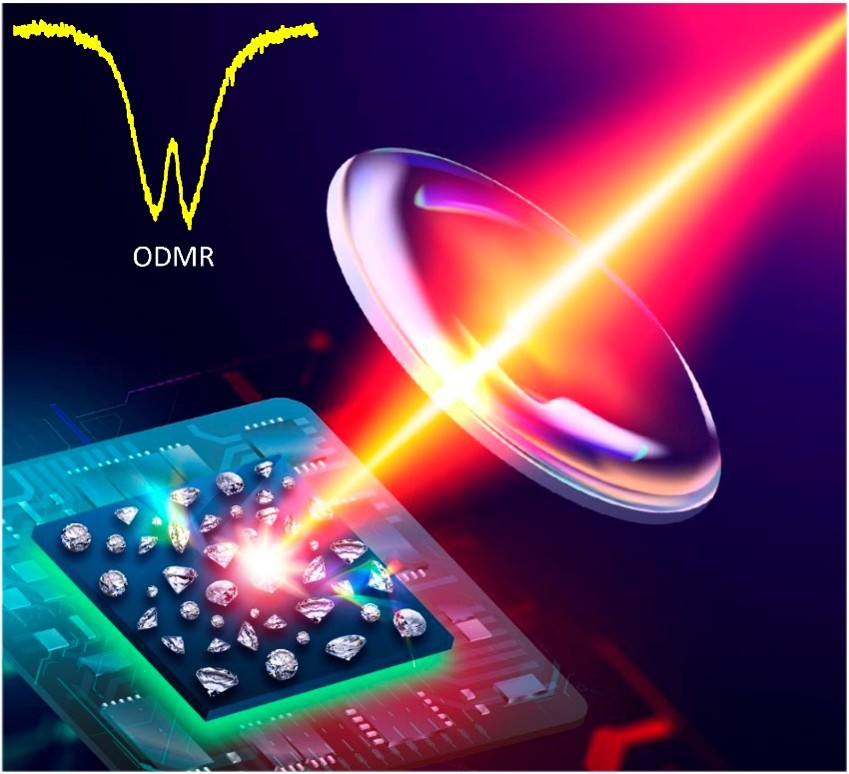
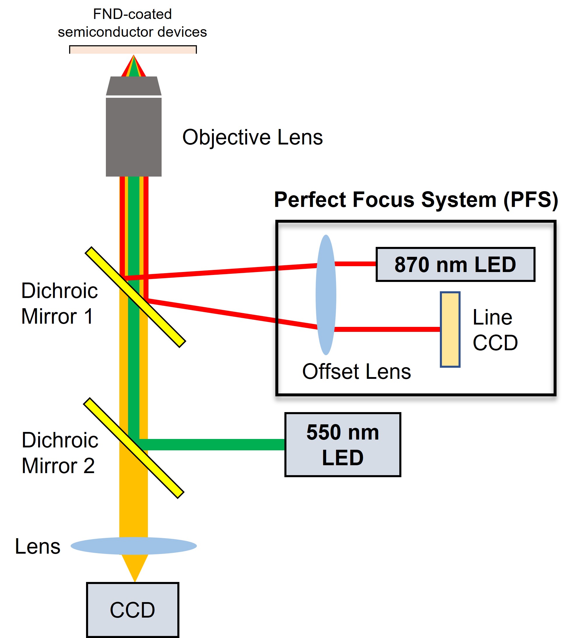
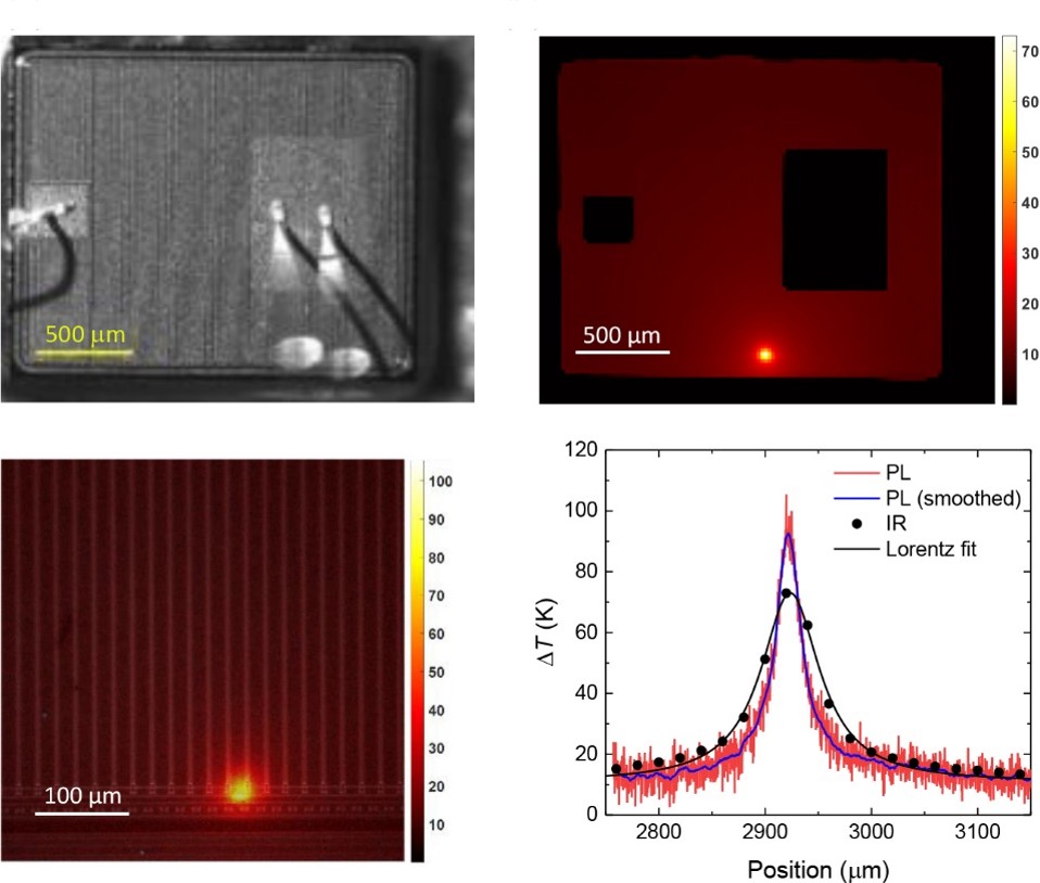
| Summary | This technology utilizes electrospray deposition to coat ultrathin fluorescent nanodiamond films onto semiconductor devices. By integrating lock-in photoluminescence thermography and optically detected magnetic resonance, it enables nanoscale, real-time temperature and magnetic field sensing of operando devices. Achieving a hotspot localization precision of 30 nm, the method outperforms conventional infrared thermography, clearly demonstrating the advantages of quantum sensing technology. |
||
| Scientific Breakthrough | Pioneering electrospray deposition of fluorescent nanodiamond (FND) quantum probes onto semiconductor chips, we have established a high-resolution, real-time monitoring platform capable of dynamically tracking thermal variations without point-by-point scanning or tedious calibration. Outperforming infrared thermography, it boosts localization precision 100-fold down to the nanoscale. This accessible and high-precision platform offers an innovative diagnostic solution for thermal management. |
||
| Industrial Applicability | Targeting advanced semiconductor thermal management and leakage localization, this technology provides a non-destructive, real-time, high-resolution failure-analysis tool. It enables nanoscale hotspot detection for both pre-packaging wafer-level defect screening and post-packaging thermal evaluation under real loads. Capable of upgrading or replacing current IR thermography, it helps foundries and IC designers shorten R&D cycles and significantly boost manufacturing yields. |
||
- Contact
- Yi-Mu Tsui
- wq001407@gmail.com
other people also saw