

| Technical Name | CFETs and beyond | ||
|---|---|---|---|
| Project Operator | National Taiwan University | ||
| Project Host | 劉致為 | ||
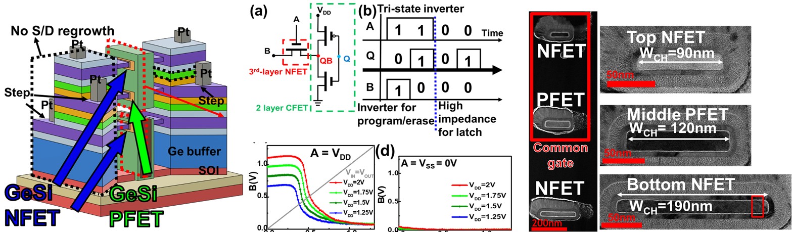
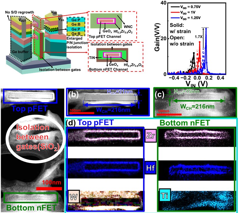
| Summary | Transistor stacking is a key approach for extending advanced technology nodes. This technology demonstrates monolithic split-gate CFETs and 3-tier transistor stacking for design flexibility and area scaling. By enabling independent gate control and 3-tier transistor stacking, it improves circuit flexibility, supports threshold-voltage tuning, and realizes half-SRAM and tri-state inverter circuits with potential for advanced logic transistors. |
||
| Scientific Breakthrough | This technology pioneers monolithic split-gate CFETs and 3-tier transistor stacking, avoiding the high cost of wafer bonding while overcoming circuit-design limits of inverter-based CFETs. It enables extreme area scaling in a monolithic process. With different work-function metals, the threshold voltage of each stacked transistor can be independently tuned, enabling improved inverter circuits. Half-SRAM and tri-state inverter circuits were also demonstrated. |
||
| Industrial Applicability | This technology improves PPA efficiency and extends Moore's Law through monolithic transistor stacking. By using split-gate CFETs and 3-tier transistor stacking, it reduces cost, enhances design flexibility, enables threshold-voltage tuning, and realizes advanced logic devices with higher density, lower power consumption, and smaller area. |
||
- Contact
- Chee Wee Liu
- cliu@ntu.edu.tw
other people also saw