| Scientific Breakthrough |
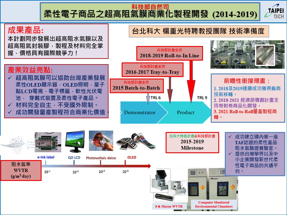
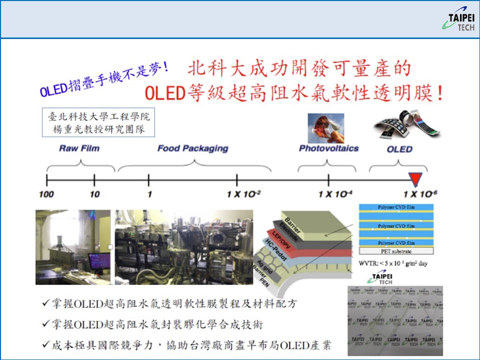
The WVTR of an uncoated plastic film is greater than 2 (g/m2/day). Depositing an inorganic coating on it, its WVTR reduces to 1~10e-1(g/m2/day). The semiconductor devices require the film of WVTR between 10e-2~10e-3(g/m2/day). To achieve the WVTR, hybrid organicinorganic layers must be coated on the substrate. Taiwan currently has no products lower than 10e-3 (g/m2/day). The barrier film of this team using hybrid multi-layer stacking makes WVTR lower than 10e-5 (g/m2/day), which is not only sufficient for photovoltaic devices but also contributes to the OLED market in the future.
|
| Industrial Applicability |
The WVTR for food packaging is between 1~10e-2(g/m2/day). Inorganic electronic products, such as light-emitting diodes, solar cells, requires WVTR around 10e-2~10e-3 (g/m2/day). The WVTR for organic electronic devices needs to be less than 10e -3(g/m2/day). OLED has the most critical one which must be lower than 10e-5 (g/m2/day). According to the UK IDTechEx forecast, from 2019 to 2029, the market value of In-Line thin-film packaging will rise from 200 million USD to 600 million USD, of which the largest demand is for OLED-related products.
|