


| Technical Name | Atomic layer technologies for advanced materialsmodules | ||
|---|---|---|---|
| Project Operator | National Taiwan University | ||
| Project Host | 陳敏璋 | ||
| Summary | With rapid evolution of Moores lawsemiconductor technology nodes down to sub-10 nm, advanced devicematerial technologies capable of Å accuracy are highly demanded. Thus we developed atomic layer technologies including atomic layer deposition, atomic layer annealing, atomic layer epitaxy,atomic layer etching, etc. for extreme control of materialsstructures with Å precision. |
||
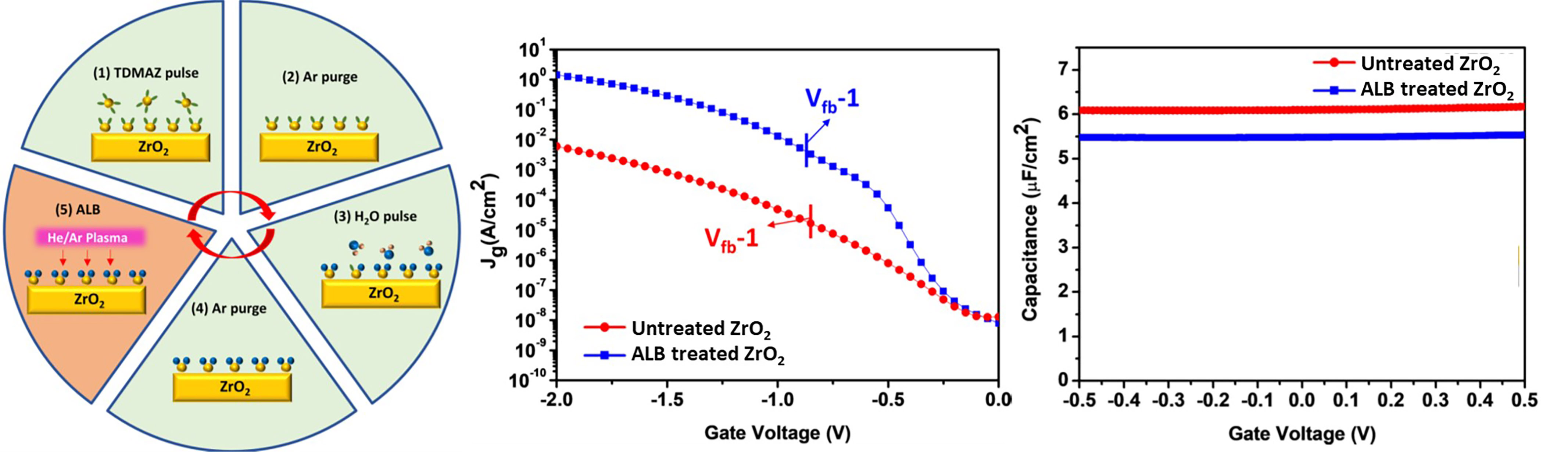
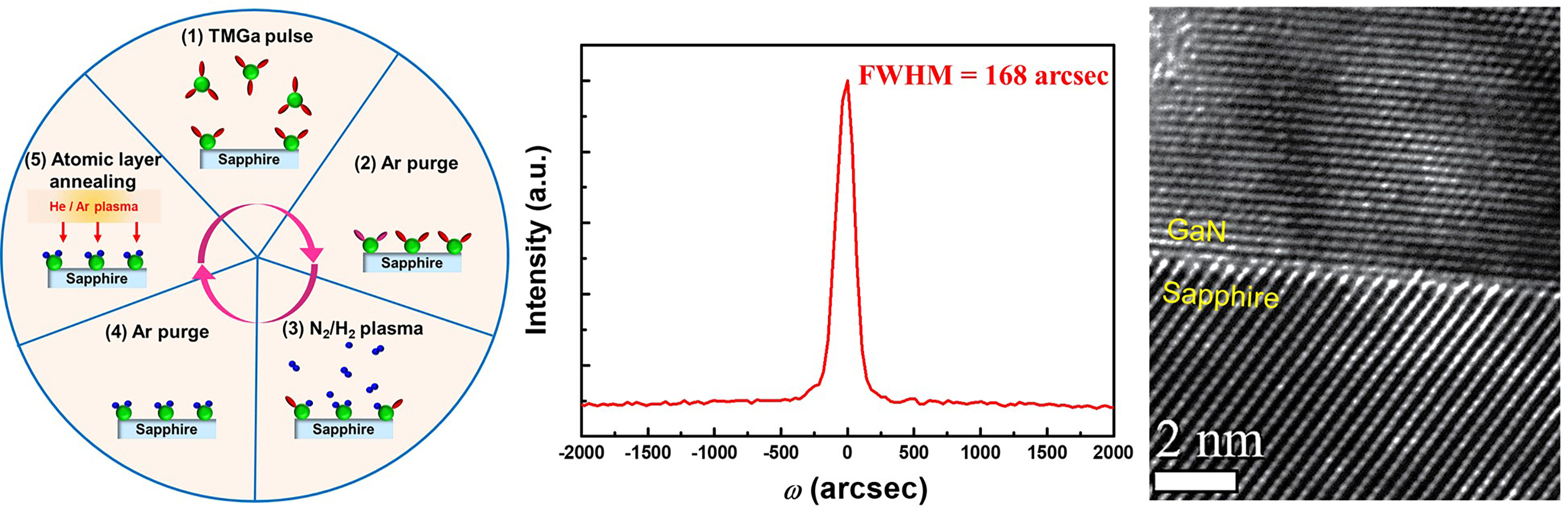
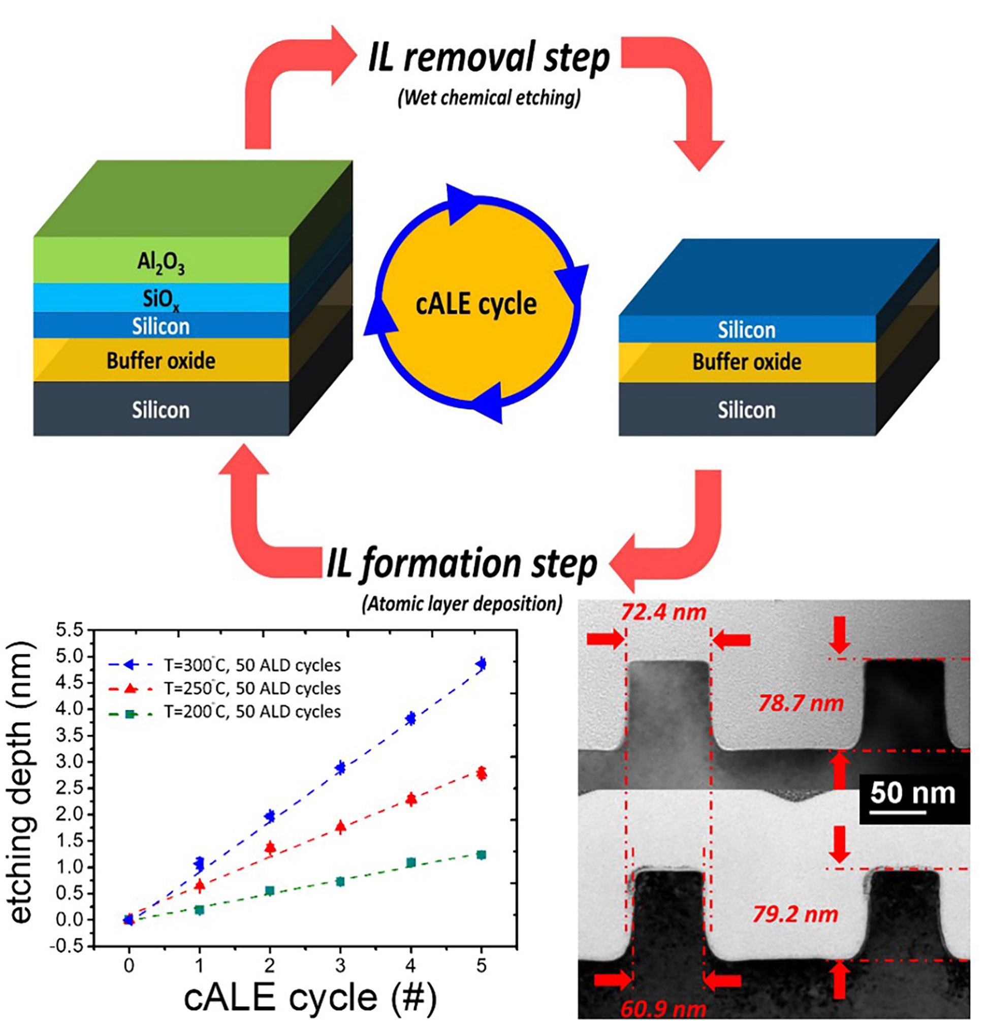
| Scientific Breakthrough | (1).Atomic layer annealing (ALA): Improvement of dielectric constant, leakage current,interfacial state density of high-K gate dielectrics. (2).Atomic layer epitaxy (ALEp): High-quality GaNAlN heteroepitaxy at a low growth temperature of only 300°C. (3).Atomic layer etching (ALEt): Self-limiting, self-stop, highly conformal, damage-free,layer-by-layer etching with Å scale accuracy. |
||
| Industrial Applicability | It is expected that the atomic layer technologies, including atomic layer deposition, atomic layer annealing, atomic layer epitaxy,atomic layer etching, etc. for advanced materialsmodules, will become key technologies for precise manufacture in sub-10 nm semiconductor technology nodesother related industries in the near future. |
||
| Keyword | Atomic layer technologies atomic layer deposition atomic layer annealing atomic layer epitaxy atomic layer etching low-temperature GaN and AlN heteroepitaxy area-selective atomic layer deposition nanolithography ferroelectric thin films negative capacitance | ||
- d9806110@gmail.com
other people also saw