
| Technical Name | MICAtronics: A Universal Platform for Fabricating Atomically Flat Single-Crystal Metal and Oxide Films | ||
|---|---|---|---|
| Project Operator | National Tsing Hua University | ||
| Project Host | 朱英豪 | ||
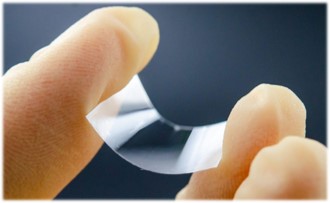
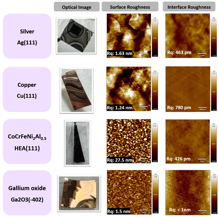
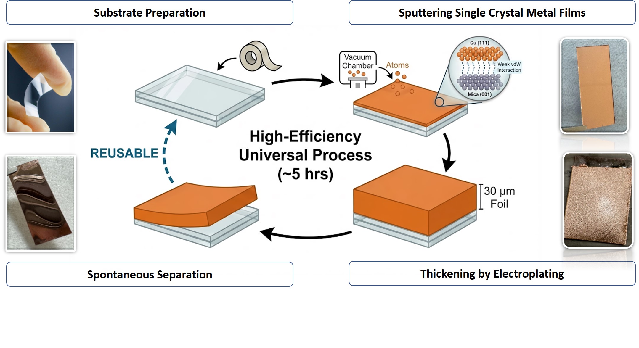
| Summary | Centering on the Micatronics platform, this technology utilizes the van der Waals epitaxy and flexibility of mica to develop atomically smooth, high-quality single-crystal thin films, including metals (Cu, Ag, Pt, Co, Ni, HEA) and oxides (ZnO, β-Ga2O3). Through electroplating and spontaneous exfoliation, we achieve a large-area, transferable single-crystal platform that significantly enhances 2D material and semiconductor performance while drastically reducing costs. |
||
| Scientific Breakthrough | This technology integrates vdW epitaxy and spontaneous exfoliation to create an atomically smooth Micatronics platform. Unlike costly, size-limited commercial single-crystal foils, our method leverages mica’s dangling-bond-free surface to bypass lattice mismatch, producing large-area metal and oxide films with bulk-like quality. By utilizing stress-controlled delamination, we ensure damage-free transfer and substrate reusability, drastically cutting costs for next-gen heterointegration. |
||
| Industrial Applicability | This technology provides large-area single-crystal metal and oxide platforms for semiconductor packaging, 2D materials, 6G THz communications, and power devices. It enhances Cu–Cu bonding reliability by reducing IMC formation, and serves as an epitaxial substrate for 2D materials. Atomically flat surfaces reduce high-frequency signal loss and scattering. It also improves heat dissipation in Ga2O3 devices via copper backplanes, enabling a low-cost and scalable heterogeneous integration platform. |
||
- Contact
- Tzu-Ming Chan
- mason10512@gmail.com
other people also saw