


| Technical Name | 與CMOS技術完全整合無須額外光罩高效節能低成本的新型態「介電質熔絲潰單次編程記憶體晶片」 | ||
|---|---|---|---|
| Project Operator | National Central University | ||
| Project Host | 謝易叡 | ||
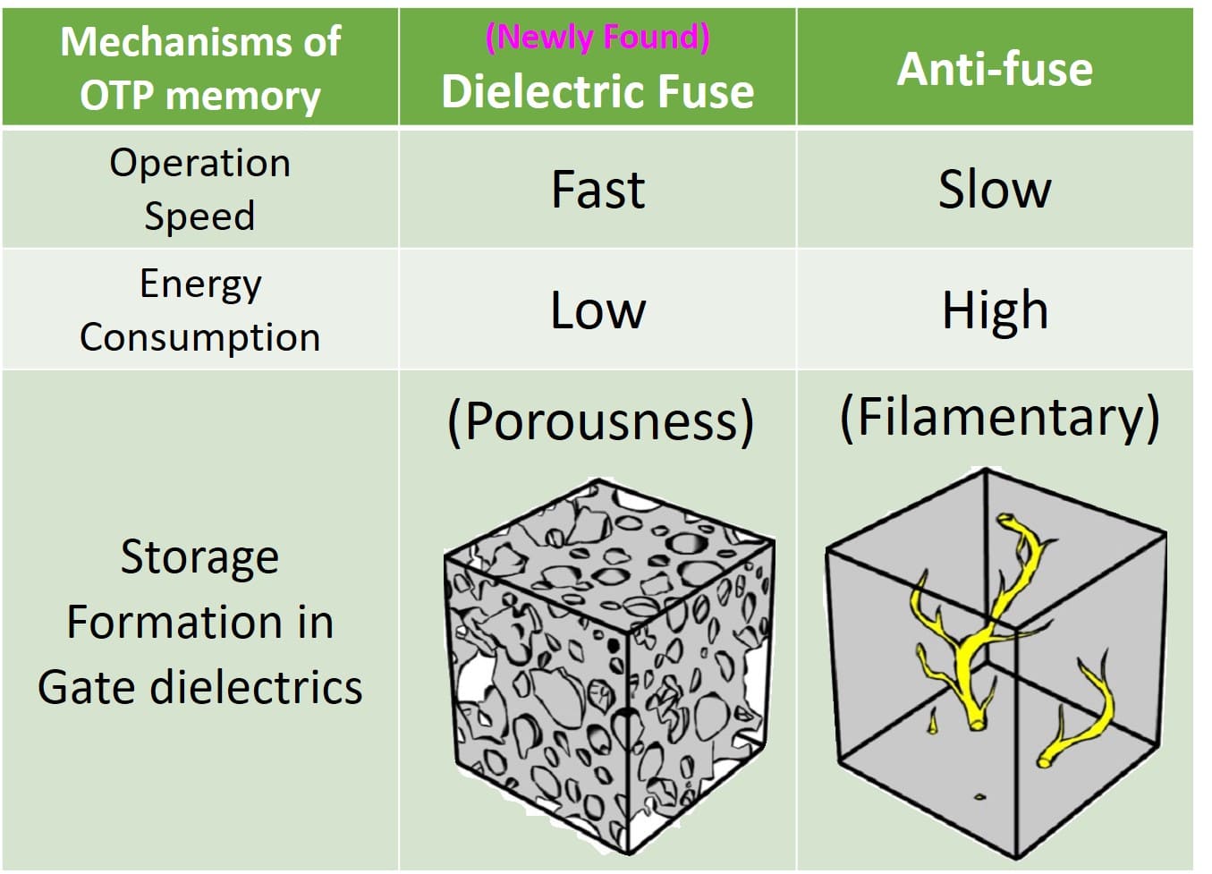
| Summary | "Introduce dielectric-fuse breakdown OTP (dFuse-OTP) technology: a.) dFuse is a newly discovered OTP mechanism which is totally different from the conventional mechanisms of anti-fuse, eFuse,charge-storage b.) IPs of dFuse OTPs have been protected globally c.) dFuse OTPs are totally integratedcompatible in the standard CMOS technologies without any additional masks d.) small layout celllow cost e.) dFuse OTPs have been at the phase of trial production in the first two big Taiwanese foundries." |
||
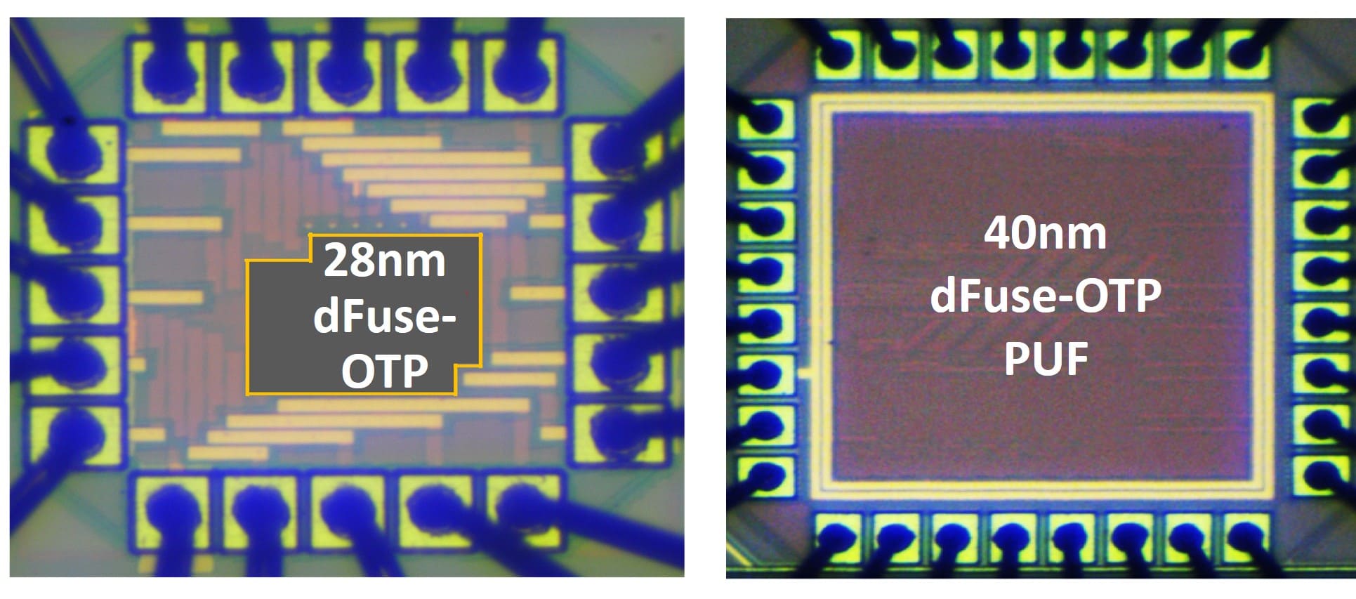
| Scientific Breakthrough | Breakthroughs of the dFuse OTPs: 1. The programming voltage 3 volts 2. The programming speed 1 micro-second 3. The programming speed 20 nano-second 4. The memory window 100 thousand times 4. The programming voltage is irrelevant to the environmental temperature 5. Life-time prediction over 10 years in 150 Celsius 6. Successful trial production on 40/28nm OTP chips 7. Bit-error-rate is approaching 0. |
||
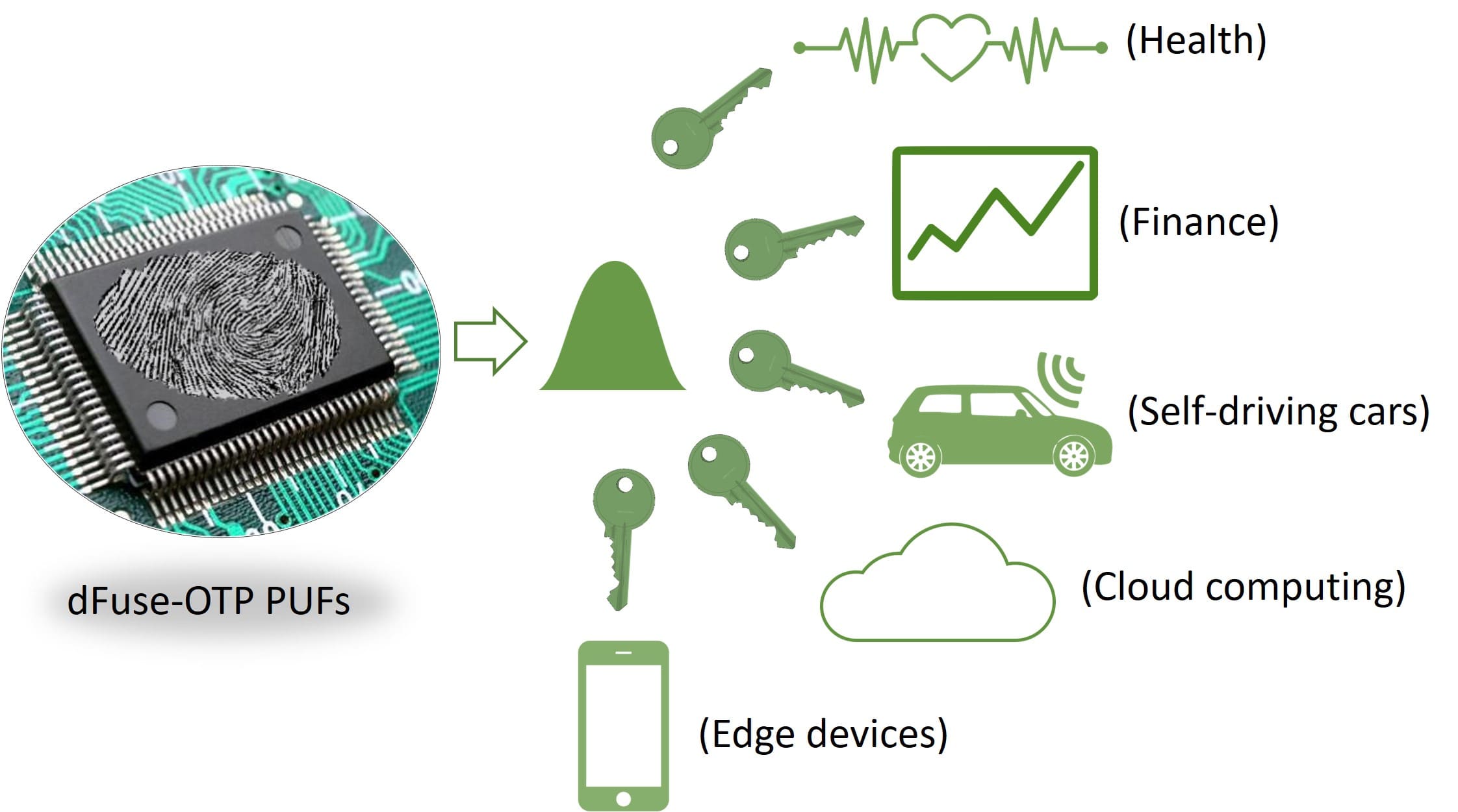
| Industrial Applicability | "Significance of the dFuse OTP PUFs on the market: a.) Security Threatens according to the raising of 5G-driving AIoT applications b.) Security becomes an important industry-supported from the worldwide nations c.) PUFs are the core hardware component of the security industry d.) OTP-based PUGs are the mainstream solution on the present market e.) our 40nm dFuse-OTP PUF exhibits excellent properties of the 0/1 MOSAIC figure, intra-HD, inter-HD,WD, compared to the industrial standards." |
||
| Matching Needs | 天使投資人、策略合作夥伴 |
||
| Keyword | OTP one-time-programming-memory embedded memory NVM AI IOT Security PUF physical-uncolonable-memory 5G | ||
- erayhsieh@cc.ncu.edu.tw
other people also saw


