


| Technical Name | 成長於低阻SiC基板上之常關型p-GaN HEMT利用AlGaN cap層實現高閘極可靠度表現 | ||
|---|---|---|---|
| Project Operator | Chang Gung University | ||
| Project Host | 邱顯欽 | ||
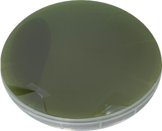
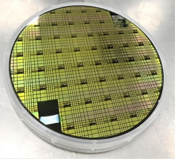
| Summary | We grew p-GaN HEMT on a low-resistance SiC substrateadded a AlGaN cap layer above the p-GaN layer. We use the wide band gap material AlGaN as the cap layer, which can effectively suppress the holes injectionachieve the purpose of improving the gate reliability. In addition, we chose a zero-degree anglelow-resistance SiC substrate, which not only greatly reduces the lattice dislocation defects caused by the heterogeneous junction, but also greatly reduces the overall cost. |
||
| Scientific Breakthrough | In this research, AlGaN capzero-anglelow-resistance SiC substrates are the first to be applied to p-GaN HEMT,our team combined the two to successfully develop a new high-voltage, high-stability p- GaN HEMT structure. |
||
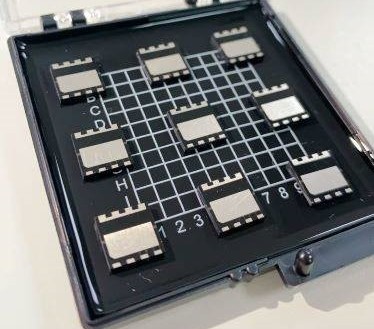
| Industrial Applicability | We grew AlGaN on the p-GaN layer to reduce the hole injection effectmake the gate operation bias20V. It is hoped that the gate driver of traditional silicon devices can be shared,the operating safety voltage of the gate will be increased at the same time. In addition, we also grew p-GaN HEMT on a low-resistancezero-degree SiC substrate, so that the GaN on SiC element can have a lower lattice defect density at the buffer layer position, improve heat dissipation performance,better the quality of crystals,there are also lower prices. |
||
| Matching Needs | 天使投資人、策略合作夥伴 |
||
| Keyword | P-type Gallium nitride High electron mobility transistor Low-resistance SiC substrate Lattice matching Thermal conductivity Low cost Gate reliability Gate turn-on voltage | ||
- hcchiu@mail.cgu.edu.tw
other people also saw


