


| Technical Name | 轉移奈米結構的方法及具有奈米結構的裝置 | ||
|---|---|---|---|
| Project Operator | Taiwan Instrument Research Institute, National Applied Research Laboratories | ||
| Project Host | 蔡淑如 | ||
| Summary | Devices with physical flexibilitystretchability have attracted a great deal of interest for use in wearable electronic technologylarge-area electronics, including displays, energy harvesters, energy storage devices, distributed sensor networks,Internet of Things applications. The present invention relates to methods for growingtransferring single-crystal III-nitride nanorodstwo dimensional transition metal dichalcogenides (2D TMDs) nanostructures,devices having the transferred nanostructures for flexible device, microLED,3DIC fabrications. |
||
| Technical Film |
|
||
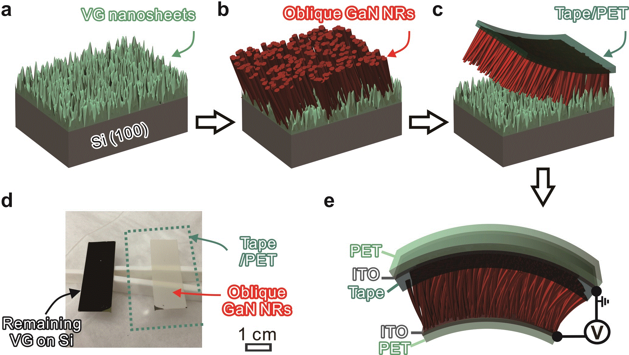
| Scientific Breakthrough | An efficient approach for growingtransferring a large area of obliquely aligned single-crystalline GaN NRs using vertically oriented graphene (VG) nanosheets was demonstrated for fabricating transparent flexible devices embedded within the transferred obliquely aligned GaN NRs. The results indicated that nanocrystalline graphene could be an excellent platform to epitaxytransfer high-quality II-VIIII-V nanostructures for flexiblethree-dimensional stacked electronics. |
||
| Industrial Applicability | An illustrative method for transferring nanostructures is provided with the steps of: forming a two-dimensional material (2D material) on a first substrate forming a plurality of nanostructures on the 2D material bonding a surface of onemore of the plurality of nanostructures with a heada second substrate, and/or shaking the onemore nanostructures withwithout a fluidseparating the onemore nanostructures from the 2D material for flexible device, microLED,3DIC applications. |
||
| Matching Needs | 1.欲媒合之產業領域:可撓式元件。2.欲媒合項目:技術合作、技術轉移、技術協助、生產製造、供應商尋找、計畫申請合作。 |
||
| Keyword | Graphene two-dimensional material nanorods nanowires transfer MicroLED Flexible device Sensors nanostructure 3DIC | ||
- sjtsai@narlabs.org.tw
other people also saw


