


| Technical Name | From IC Layout to Die Photo: Deep Learning-Based IC Fabrication SimulationMask Correction | ||
|---|---|---|---|
| Project Operator | National Tsing Hua University | ||
| Project Host | 林嘉文 | ||
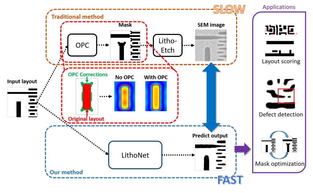
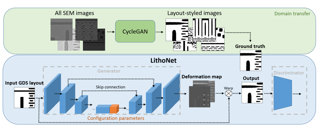
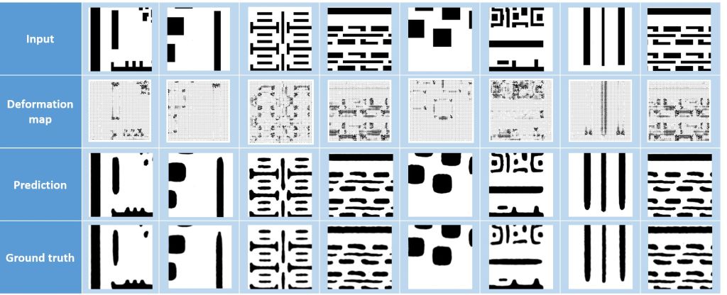
| Summary | This technology consists of two convolutional neural networks (CNNs): LithoNetOPCNet. LithoNet mimics the fabrication procedure, involving lithographyetching, to predict the shape of a fabricated IC circuitry given an input layout. OPCNet, in cooperation with a pre-trained LithoNet, mimics the optical proximity correction procedure used to correct the layout designgenerate a modif |
||
| Scientific Breakthrough | This technology is the first to use a deep neural network to accurately model the effect of lithographyetching processes on the shape deformation of a fabricated IC circuitry. It can also generates a correct mask pattern so that the fabricated IC circuitry will have a shape close to a desired pattern. The technolgy can lead to a paradigm shift of IC design for manufacturability. |
||
| Industrial Applicability | This technology can be used by semiconductor manufacturers for modeling IC fabrication processesIC design CAD tools for design for Manufacturability. |
||
| Keyword | Deep Learning Covolutional Neural Network IC Fabrication Virtual Metrology Lithography Etching Photomask correctiin Optical Proximity Correction Computer Aided Design Design for Manufacturability | ||
- jsyoaliu@gmail.com
other people also saw