


| Technical Name | Wafer Level Probing System for Semiconductor Gas Sensor with High Throughput | ||
|---|---|---|---|
| Project Operator | Taiwan Instrument Research Institute, NARLabs | ||
| Project Host | 陳峰志 | ||
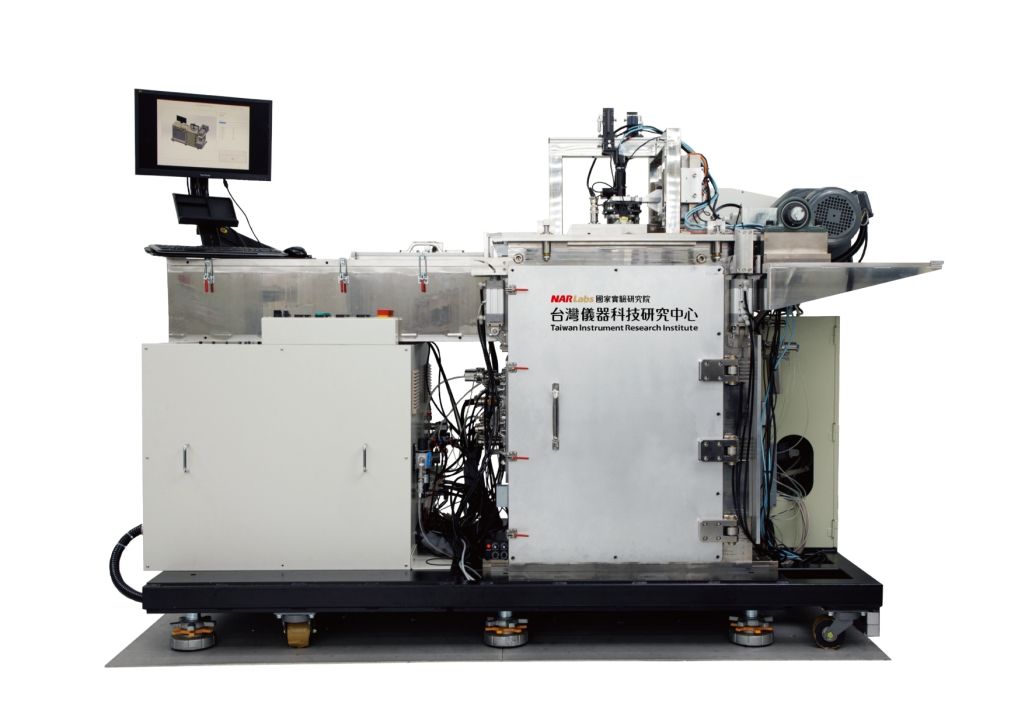
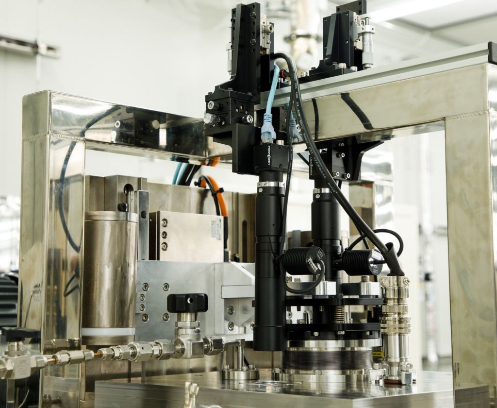
| Summary | Proposed system is integrated by an automatic optical registration system, a linear arrayed probing device, a vacuum chamber and gas supply system, a validation system of gas concentration, a chuck table combined with heating device, and precisely positioning platform. The electrical features of wafer-based gas sensor chips can be measured efficiently to check each sensor quality in advance, and unqualified chips can be discarded to avoid them getting into the following packaging processes. |
||
| Scientific Breakthrough | Proposed system is integrated by an automatic optical registration system, a linear arrayed probing device, a vacuum chamber and gas supply system, a validation system of gas concentration, a chuck table combined with heating device, and precisely positioning platform. The electrical features of wafer-based gas sensor chips can be checked in advance to avoid the unqualified chips getting into the packaging processes. |
||
| Industrial Applicability | System equipment can provide the functionality and performance measurement for wafer-based gas sensors chips. The quality for each chip can be determined before packaging, and then the testing period for sensors development can be reduced substantially. Moreover, for production phase of gas sensors, the unqualified chips can be sieved out at wafer level to reduce the waste of packaging resources. |
||
| Keyword | High-efficiency probing system wafer-based gas sensor linear arrayed probe card automatic optical registration chuck table integrated with a heating device welding bellow gas supply system vacuum chamber system precisely positioning platform system integration | ||
- yihaolin@tiri.narl.org.tw
other people also saw