

| Technical Name | Next-Generation High-Speed Electronic Materials - GaN Semiconductor Epitaxy and Process Technology | ||
|---|---|---|---|
| Project Operator | Taiwan Semiconductor Research Institute | ||
| Project Host | 許隆興 | ||
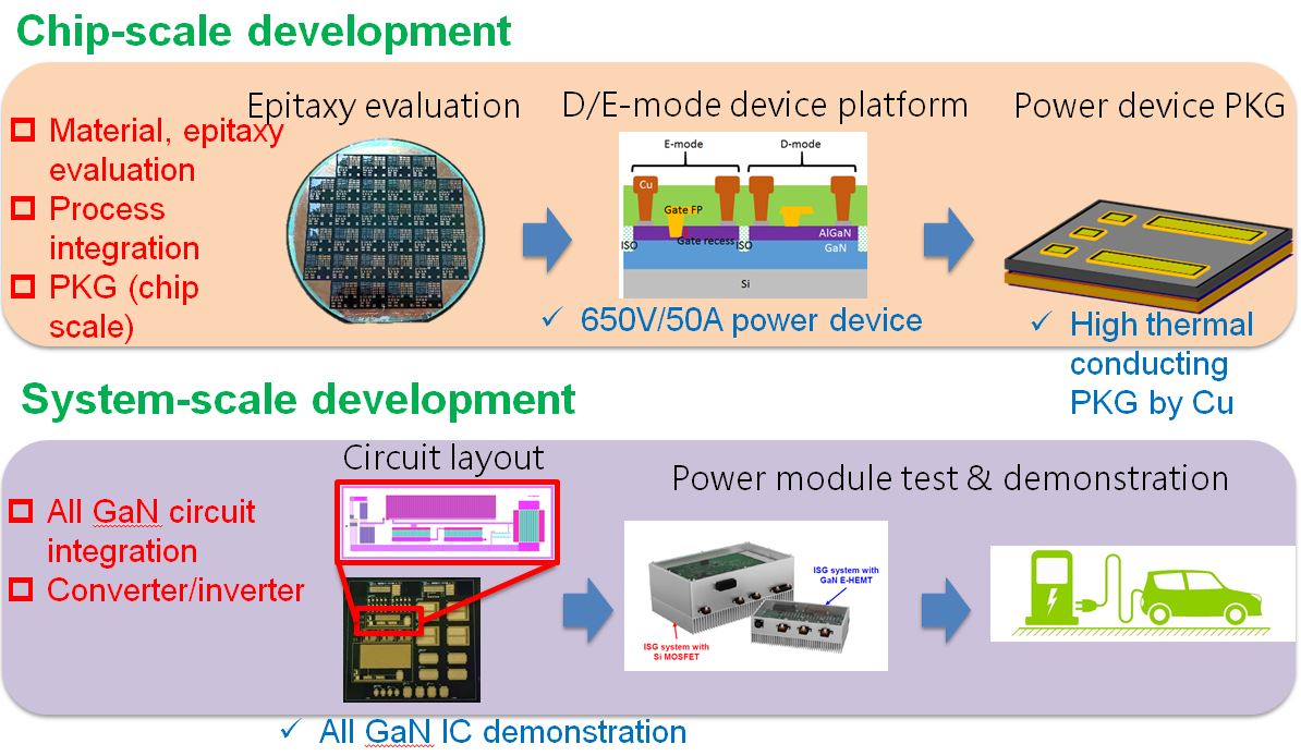
| Summary | Establishing an 8-inch GaN epitaxy center in Taiwan to provide researchers with a stable, high-quality environment for fabricating compound semiconductor wafers and devices on silicon or transparent substrates. |
||
| Scientific Breakthrough | Demonstrates the practical application and technical verification of Gallium Nitride (GaN) materials in forward-looking industries such as new energy, high-frequency power systems, and low-earth orbit satellites. |
||
| Industrial Applicability | Supports the "Great South New Silicon Valley" initiative by providing high-quality epitaxial wafers, promoting the commercialization of advanced technologies in new energy vehicles, 5G/6G communications, and LEO satellites. |
||
- Contact
- Lung-Hsing Hsu
- algerhsu@niar.org.tw
other people also saw