

| Technical Name | In-situ Raman Characterization Technology for Wafer-Scale 2D Material Chips | ||
|---|---|---|---|
| Project Operator | National Center for Instrumentation Research, NIAR | ||
| Project Host | 林郁洧 | ||
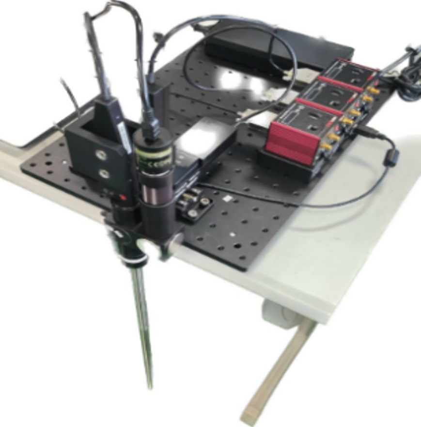
| Summary | The in-situ Raman monitoring module integrates real-time imaging and spectral acquisition capabilities. Designed with a modular architecture, it can be installed on CVD (chemical vapor deposition) systems to enable real-time monitoring of crystallographic signals during semiconductor material growth, allowing precise observation of structural formation and phase transitions in two-dimensional thin films. This technology supports atomic-scale thin-film processing and material validation, enabling the verification of in-house developed equipment and key components for next-generation manufacturing processes. It further promotes the localization and development of semiconductor equipment, critical materials, and enabling technologies. |
||
| Scientific Breakthrough | This system integrates Raman spectroscopy and real-time imaging into a modular architecture that can be directly embedded into CVD (chemical vapor deposition) process environments. It overcomes the limitations of conventional ex-situ measurement approaches, enabling in-situ, real-time monitoring of material growth processes. It also allows the simultaneous analysis of crystallographic formation and phase transitions in two-dimensional thin films, providing dynamic, atomic-scale process information. |
||
| Industrial Applicability | This in-situ Raman monitoring module can be directly integrated into CVD (chemical vapor deposition) semiconductor process equipment, providing real-time, non-destructive material monitoring capabilities during processing. It supports quality control and process parameter optimization for wafer and two-dimensional material growth, thereby improving yield and process stability. Furthermore, it can be applied to advanced materials research and process development, accelerating the validation of new materials for mass production. It also supports the performance verification of semiconductor equipment and key components, as well as the localization of critical technologies, strengthening overall supply chain autonomy. |
||
- Contact
- Wei-Chun Chen
- weichun@niar.org.tw
other people also saw