
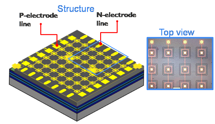
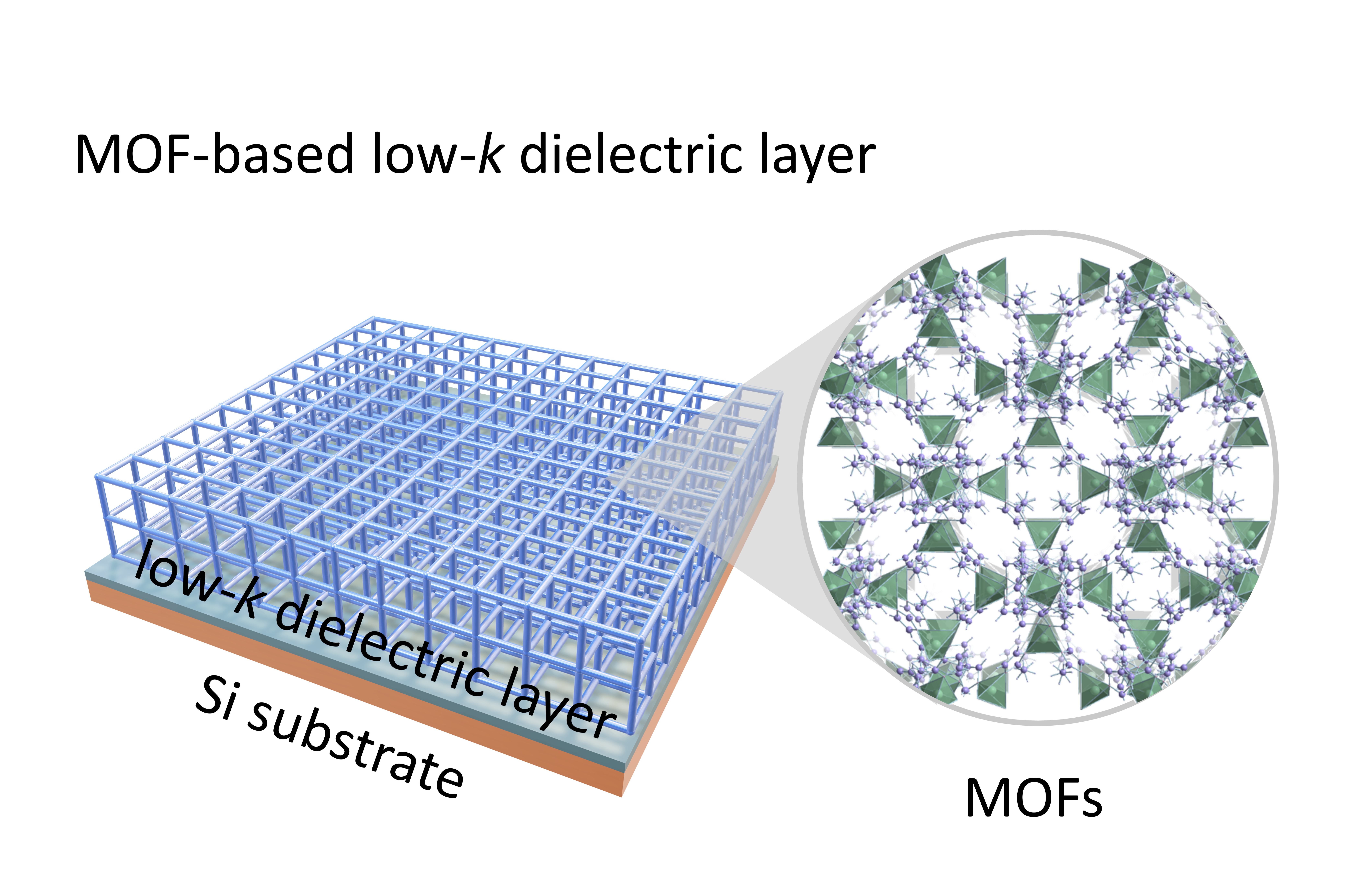
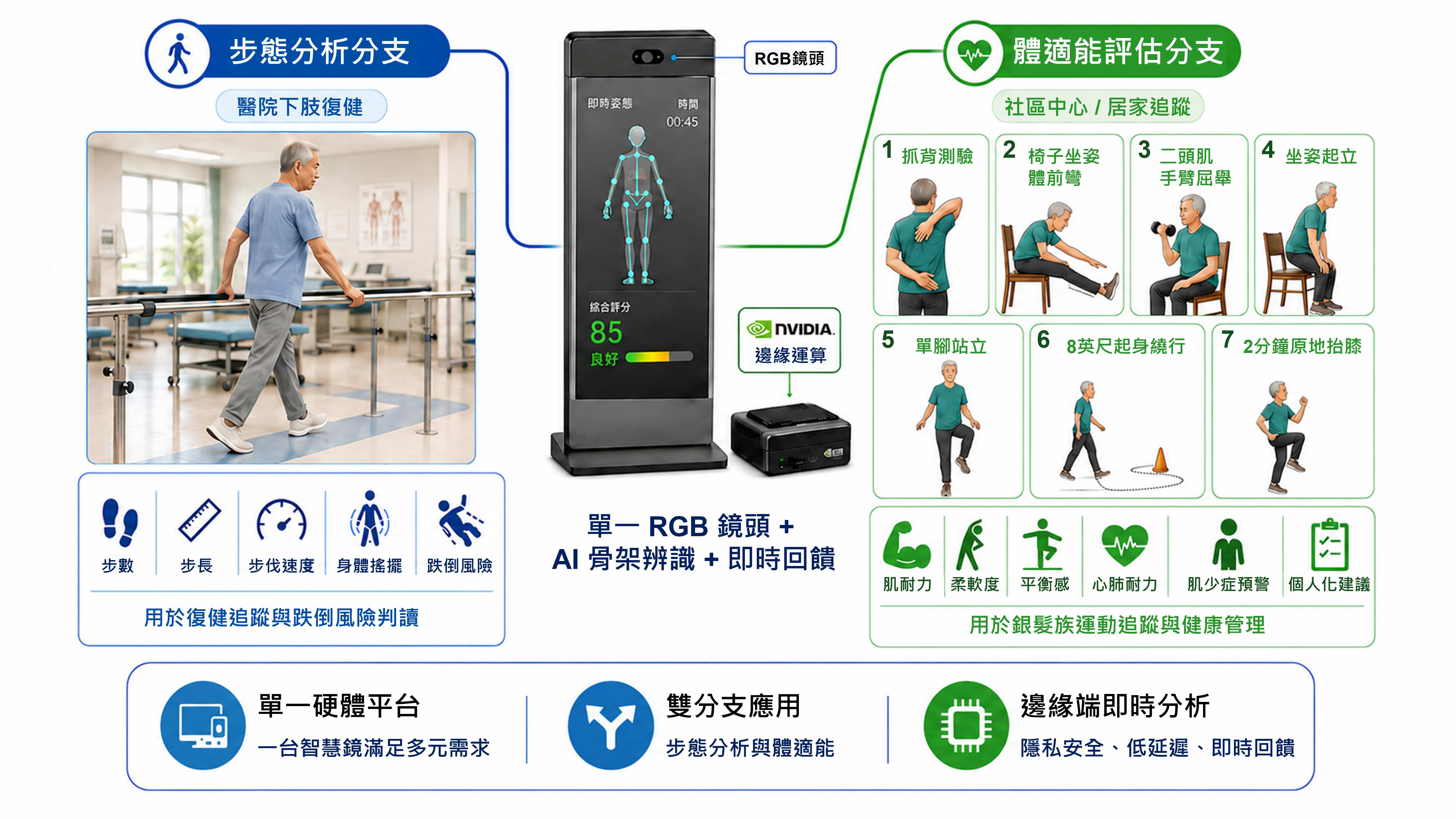
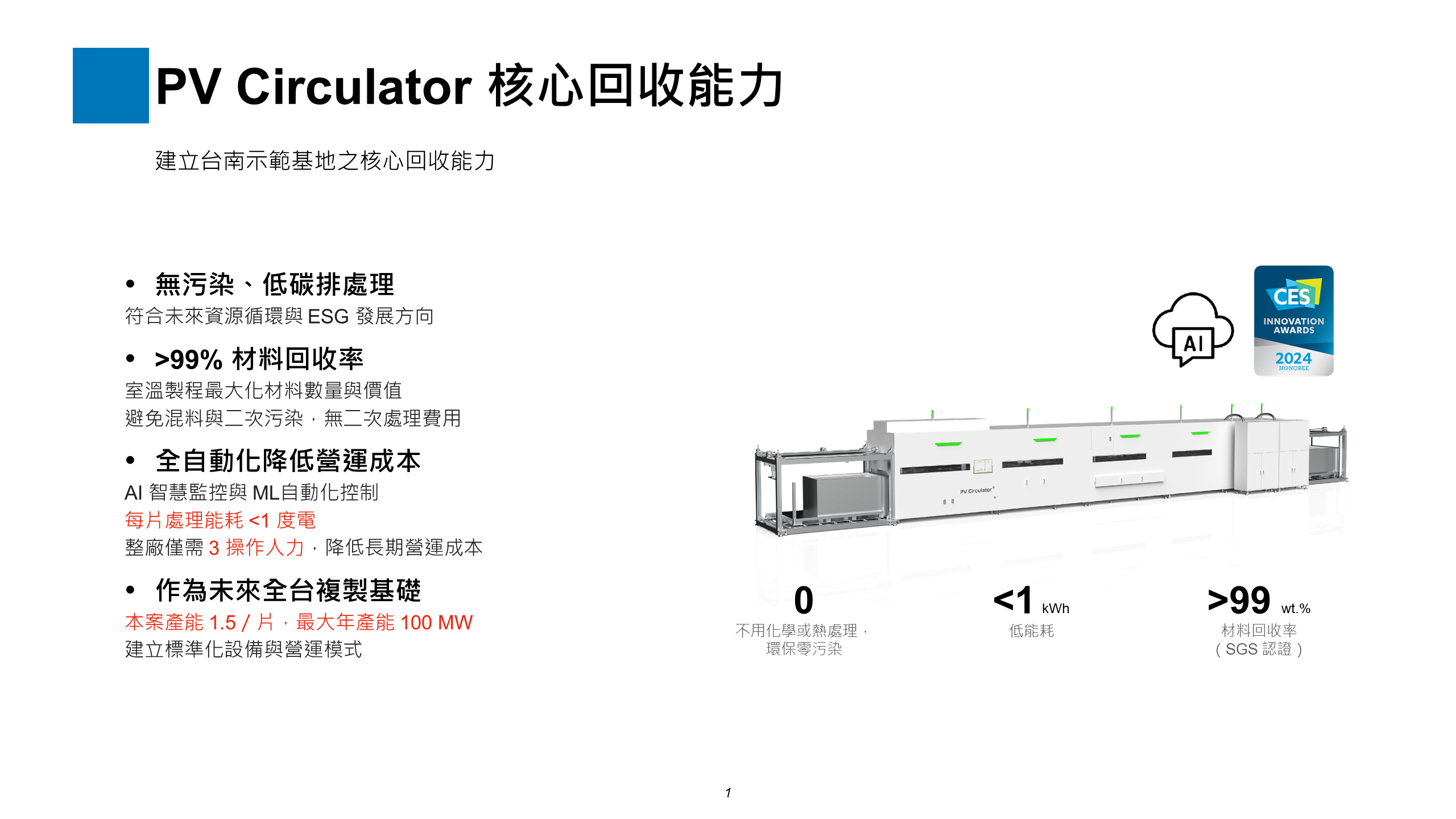
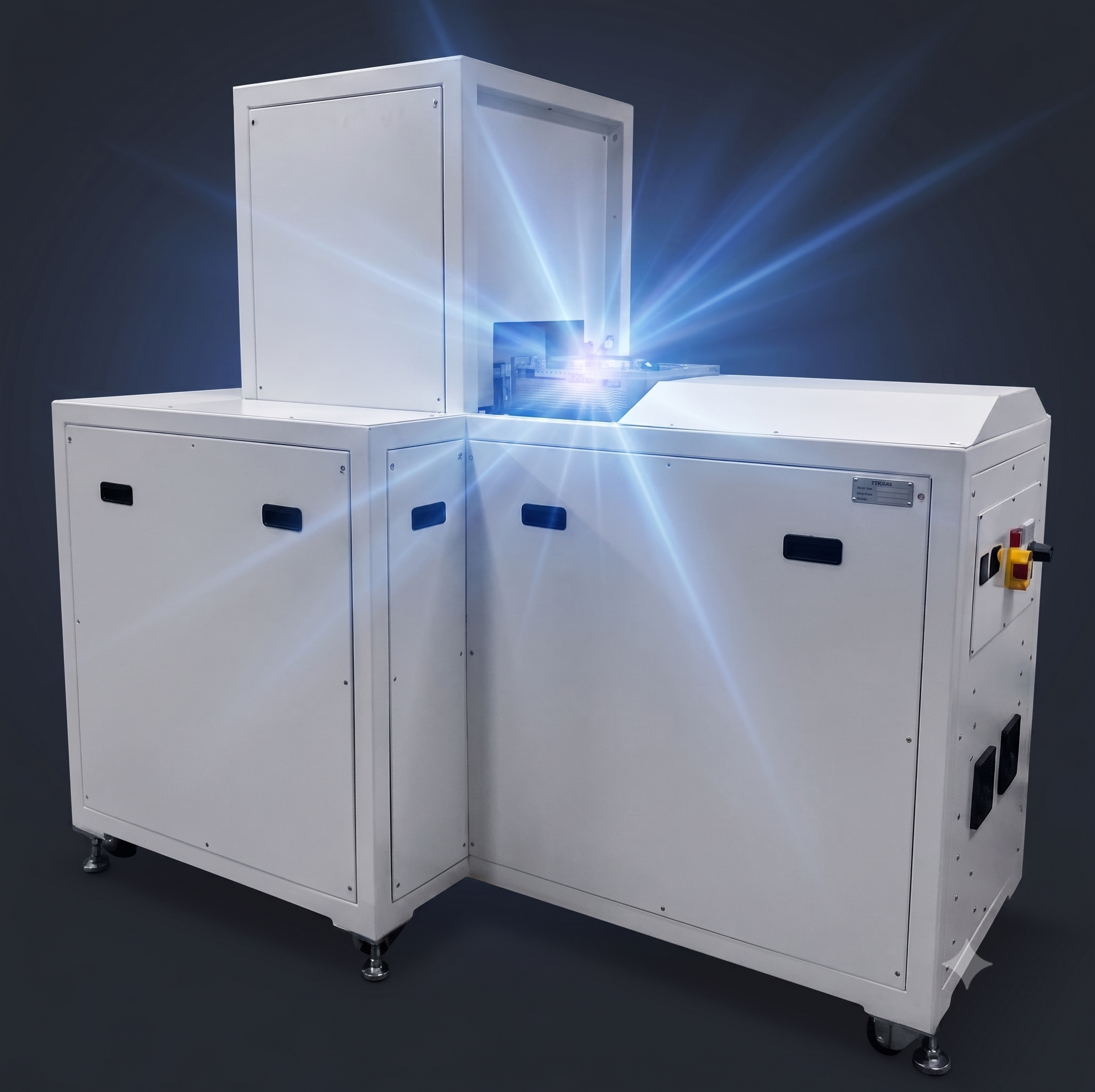
| Technical Name | Photon-Induced Atomic Layer Deposition | ||
|---|---|---|---|
| Project Operator | National Tsing-Hua University | ||
| Project Host | 邱博文 | ||
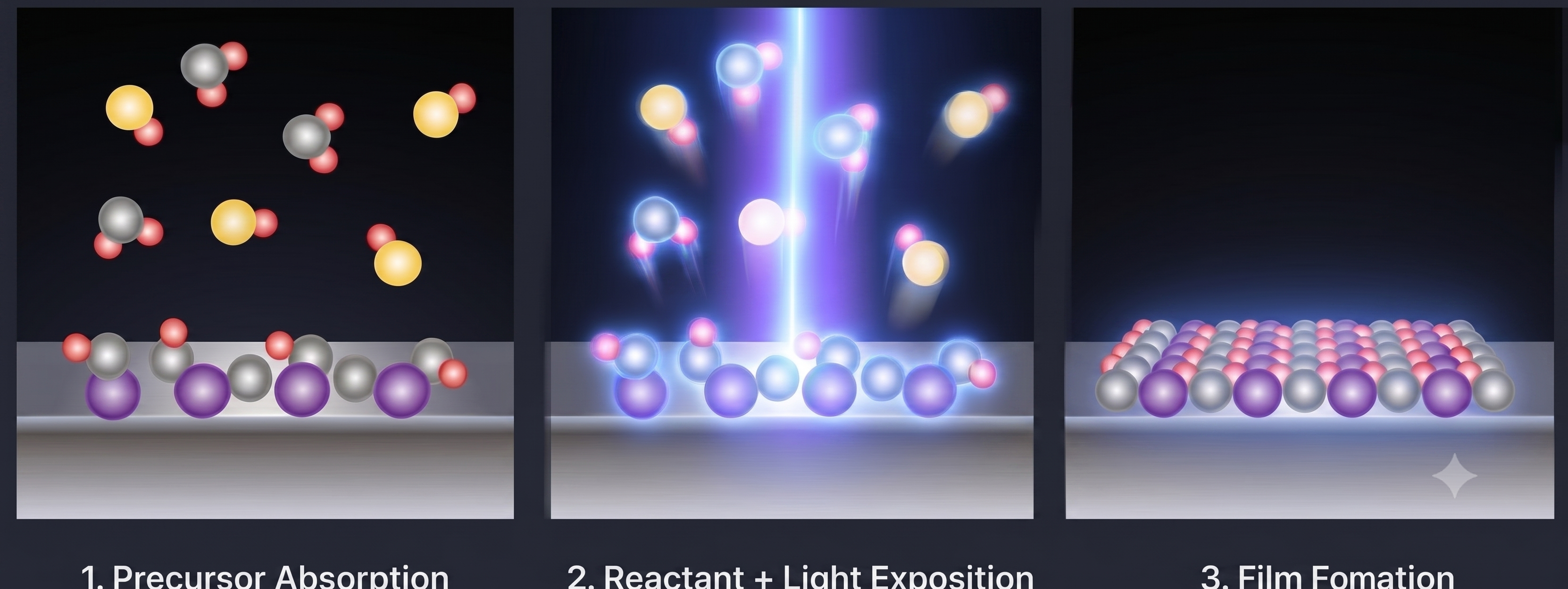
| Summary | "Photo-Induced Atomic Layer Deposition (PI-ALD) Through a proprietary mechanical design, PI-ALD stands as the world's only technology to incorporate photocatalytic reactions into material deposition. This breakthrough effectively addresses the critical process challenge of trench filling in advanced semiconductor manufacturing, while simultaneously enabling selective area deposition through precisely controlled photocatalysis — another capability unmatched globally. Thin films deposited via PI-ALD deliver a compelling combination of performance advantages: - Lower surface roughness for superior film uniformity - Reduced residual functional-group elements (e.g., carbon and oxygen) for higher film purity - Lower metallic resistivity for enhan |
||
| Scientific Breakthrough | " Photon-induced chemical reactions and atomic diffusion enable precise control of thin film deposition, eliminating void and seam defects commonly encountered during gap-fill processes Photon-induced bond dissociation of precursors and reactants significantly reduces residual functional-group impurities — including carbon (C), oxygen (O), and nitrogen (N) — thereby enhancing film quality and improving properties such as metallic electrical conductivity Multi-layer molecular adsorption technology delivers a multiplicative increase in deposition rate, dramatically improving process throughput Photon-induced radical-driven chemical deposition eliminates device damage caused by charged ions " |
||
| Industrial Applicability | Photo-induced ALD uses ultraviolet or visible light to activate precursor reactions, enabling deposition at low temperatures and achieving area-selective growth. Its major industrial applications include: selective deposition and self-aligned patterning in advanced semiconductor processes, and reduced thermal budget to protect temperature-sensitive devices; low-temperature thin-film encapsulation for flexible electronics and OLED displays; as well as photocatalysis, sensors, and transparent conductive films. Its light-controlled spatial and temporal precision aligns well with the demands for precise processing amid the trends toward heterogeneous integration and device scaling. |
||
- Contact
- Yen, Jui-Kang
- riconyen@pi2.com.tw
other people also saw