


| Technical Name | EDA tools | ||
|---|---|---|---|
| Project Operator | National Tsing Hua University | ||
| Project Host | 林嘉文 | ||
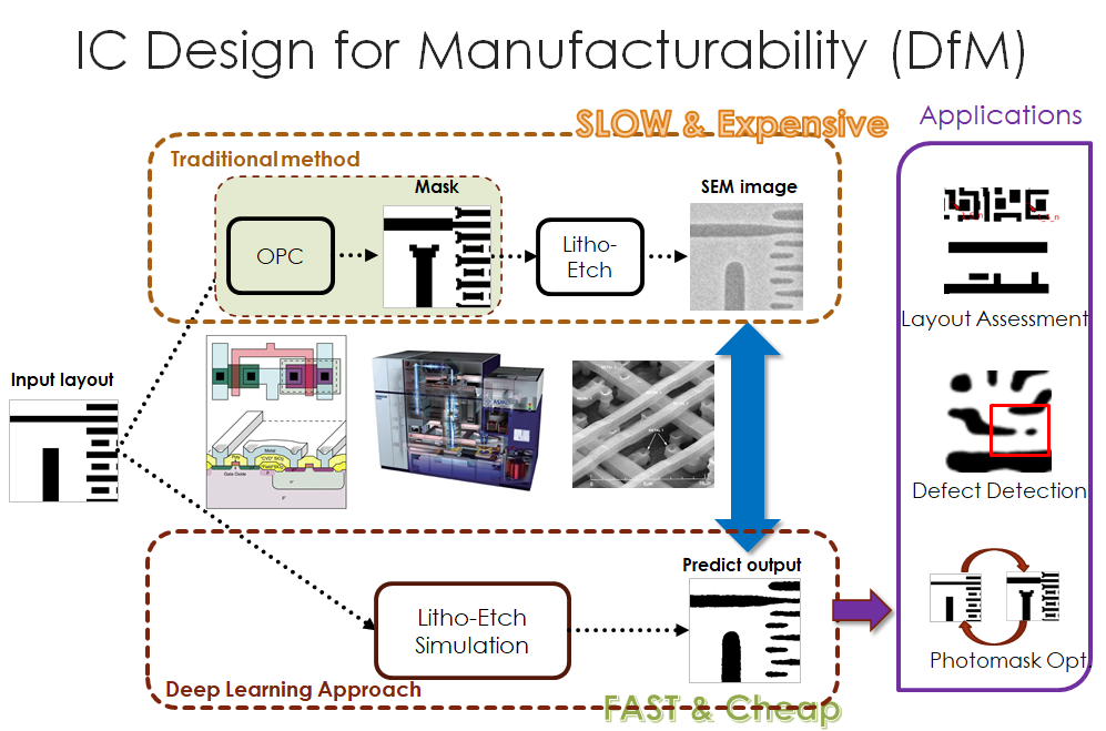
| Summary | We exploit deep learning techniques to develop EDA tools for semiconductor manufacturing. Our EDA tools can predict circuit shape distortions caused by the lithography processes and thus assess the photomask correction results at an early stage. These tools can be applied to layout's OPC simulation, layout hotspot detection, IC defect detection, and photomask optimization. |
||
| Scientific Breakthrough | This is the world's first technology that uses computer vision techniques to accurately predict the distortions on IC circuits caused by lithography processes, significantly surpassing current EDA design tools. It is expected to lead to a paradigm shift in semiconductor process EDA. |
||
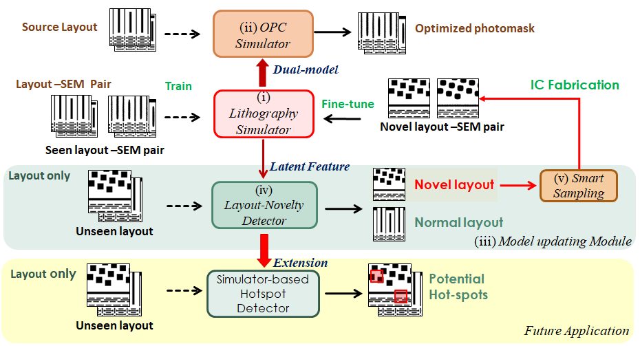
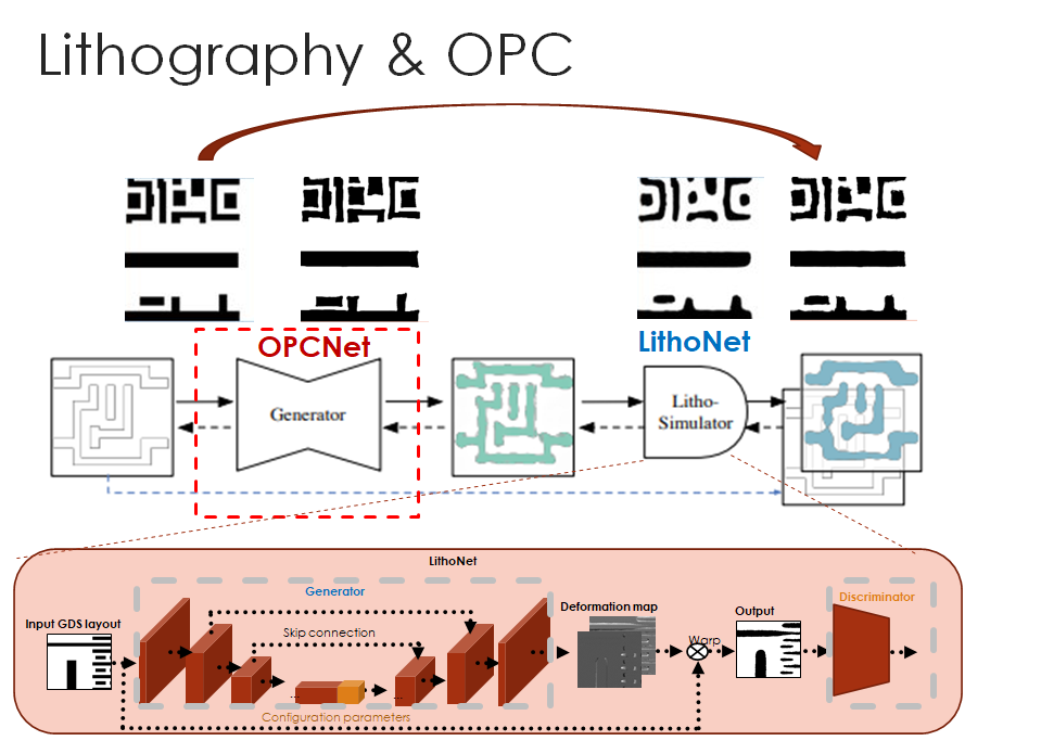
| Industrial Applicability | This technology is a collaborative achievement with United Microelectronics Corporation. Its features include: (1) It's the world's first computer vision based system able to predict the IC circuit distortions, caused by lithography processes, with a speed surpassing commercial software. (2) It can be utilized as an OPC tool for correcting layout photomask patterns. (3) This model can identify novel layouts, which can subsequently be used to refine the model. In sum, this technique is expected to lead to a paradigm shift in EDA. Parts of our achievements have been published in two IEEE T-CAD papers. |
||
- Contact
- Shao, Hao-Chiang
- shao.haochiang@gmail.com
other people also saw