


| Technical Name | 3D Atomic Electron Tomography for Advanced Electronic Devices | ||
|---|---|---|---|
| Project Operator | National Tsing Hua University | ||
| Project Host | 陳健群 | ||
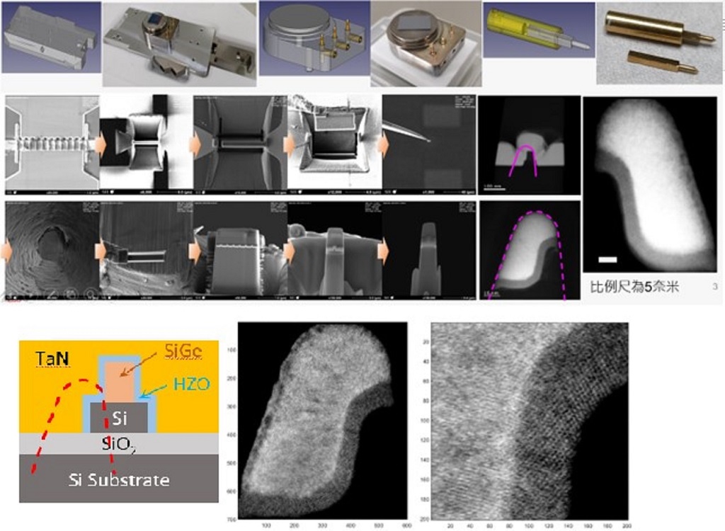
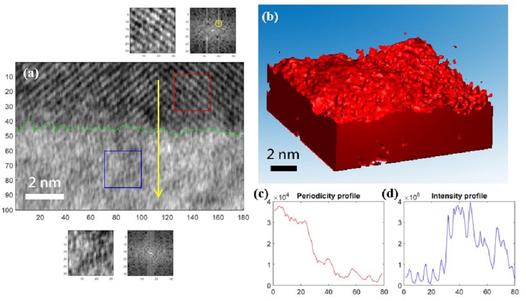
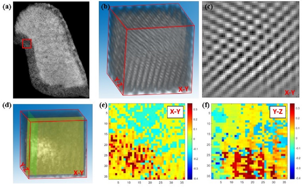
| Summary | This technology combines needle-shaped sample preparation with focused ion beams, spherical aberration-corrected electron microscopy,tomographic reconstruction technology to obtain non-destructive 3D transistor atomic structures with a resolution of 1.8 angstroms. This approach can calculate 3D atomic structure, 3D sidewall roughness, 3D element distribution,3D stress distribution in the transistor, providing a new inspection vision for advanced componentsrelated processes. |
||
| Scientific Breakthrough | Current literature regarding 3D atomic imaging is mainly proof-of-concept articles using nanoparticles,this technology has not been extended to semiconductor samples because the sample preparation is too complicated. Our team reports the first demonstration in the world analyzing the 3D atomic structure, 3D interface roughness, 3D element,stress distribution non-destructively of an advanced transistor with a resolution of 1.8 angstroms. |
||
| Industrial Applicability | The team independently develops this technology without foreign assistance. Also, we have completed TSMC's trial sample to clarify its industrial applicability. The automation of atomic-level image collection3D reconstruction combined with graphics processing unit (GPU) calculations will speed up the completion of cases that initially take one month to one day, achieving feasiblequantifiable industrial application possibilities. |
||
| Keyword | Atomic Electron Tomography finFET spherical aberration-corrected electron microscope 3D atomic structure 3D element distribution 3D atomic strain distribution 3D interface roughness | ||
- Contact
- Chen, Chien-Chun
- ccchen0627@gmail.com
other people also saw