


| Technical Name | Large-area, high-efficiency, CMOS-compatible metalenses | ||
|---|---|---|---|
| Project Operator | National Yang Ming Chiao Tung University (NYCU) | ||
| Project Host | 余沛慈 | ||
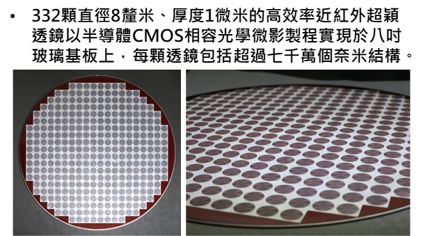
| Summary | We successfully use low-cost photolithography with standard CMOS processes to fabricate 332 high-efficiency near-infraredvisible metalenses with 8 mm diameter on an 8-inch glass substrate. Each metalens contains over 70 million nanostructuresachieves a conversion efficiency close to the diffraction limit. Our technology enables mass-producing metasurfacesmetalenses at low costallows the integration of opticalelectronic components in miniature CMOS image/depth sensors. |
||
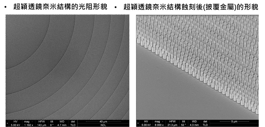
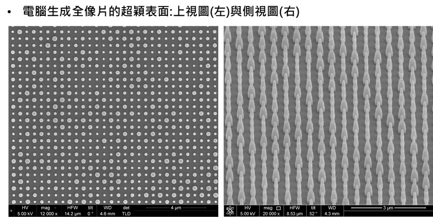
| Scientific Breakthrough | This work presents large-area near-infraredvisible metalenses produced with today’s semiconductor CMOS processes. Through low-cost photolithographyresolution enhancement technology, we can precisely control the dimensions of nanopillars in the metalens to achieve diffraction-limited focusing with high efficiency. The work will enable the integration of metalensmetasurfaces into CMOS sensors, allowing versatile optoelectronic componentssystems in a miniature form. |
||
| Industrial Applicability | The rise of the metaverse in recent years has driven the development of wearable devices related to virtual reality (VR)augmented reality (AR). Metasurfacesmetalenses that can manipulate electromagnetic waves in a very small form factor have shown promising potential to replace traditional optical components for metaverse applications. The CMOS-compatible processes further permit the integration of opticalelectronic components in tiny IC chipssensors. |
||
| Keyword | Metalens Metasurface Photolithography mass-production optical proximity correction deep learning metaverse augmented reality virtual reality mixed reality | ||
- Contact
- Ligen Chiu
- ligen@mail.nctu.edu.tw
other people also saw