


| Technical Name | Enhancing Anodization of Semiconductor Materials Technology with Wafer Bonding Transforming Interface Function | ||
|---|---|---|---|
| Project Operator | National Central University | ||
| Project Host | 李天錫 | ||
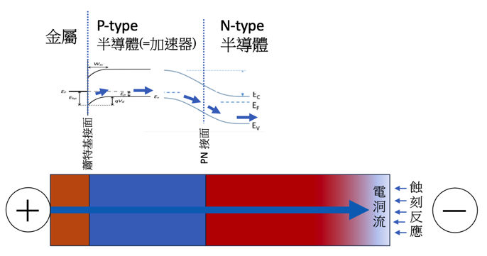
| Summary | Electrochemical process utilizes the injection of holes to induce surface atomic dissociation for etching. Implementing it in N-type semiconductors is challenging due to the lack of holes. This technique utilizes wafer bonding, where N-type silicon carbide is bonded to P-type silicon to form a PN junction, enhancing reaction efficiency by manipulating the interface to facilitate hole injection. After etching, the P-type silicon can be removed to be extended to other N-type semiconductors. |
||
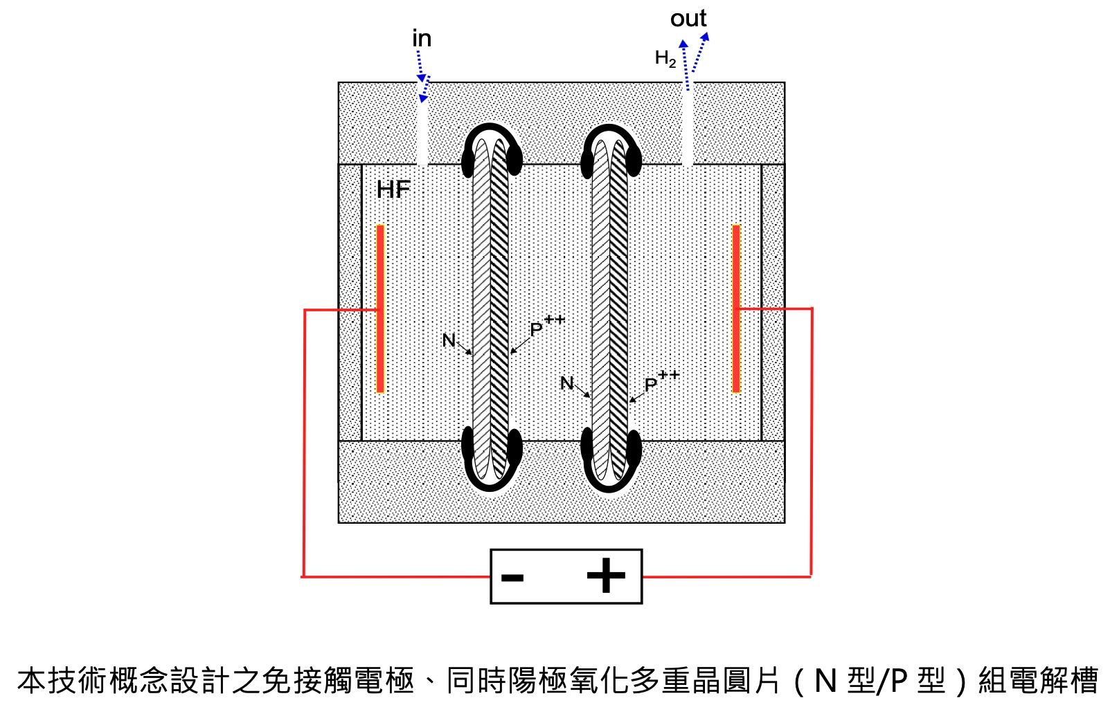
| Scientific Breakthrough | Detachable PN junction is created by placing P-type Is as an intermediate electrode to accelerate electrochemical etching. This approach avoids doping contaminationexpensive operations,it can be applied to various N-type semiconductors. A contactless electrode electrochemical device can be developed, where P-type Is injects holes into the N-type semiconductor, enabling multiple electrochemical reactions simultaneously. The technology increases efficiency in formation more than 200. |
||
| Industrial Applicability | The substrate accounts for 55 of the production cost of silicon carbide components. It is predicted that the production of electric vehicles will reach 50 million in 2027, requiring 25 million SiC wafers. Accelerated thinning is an important technology development direction. This technology uses wafer bonding to adjust the interface function, transforming the carrier flow into an injective "dominant current". The acceleration can expand the market share of cutting, grindingpolishing. |
||
| Keyword | Silicon Carbide Speed-up Reaction Schottky Junction PN Junction Wafer Bonding Hole-Input Electron-Sink Electrochemical Thinning Detachable and Reuse Type III Semiconductor | ||
- Contact
- You-Sheng Qiu
- kiuc741852@gmail.com
other people also saw