


| Technical Name | High mobility materials, process, stacked channels,thermal circuit simulation Ferroelectric X:HfO2 for Negative CapacitancePOC(Proof-of-Concept) Applications Atomic layer technologies for | ||
|---|---|---|---|
| Project Operator | National Taiwan University – TSMCxNTU Joint Research Center | ||
| Project Host | 劉致為 | ||
| Summary | "1.High mobility Ge channel stacked gate-all-around transistors 2.Fabrication of 3-D NCFETs, corresponding module development, ferroelectric tunneling memristor for neuromorphic computing,the co-simulation between embedded memorydevices 3. Circuit level thermal-electrical SPICE modeling, providing the junction temperaturethe temperature distribution in the metal lines for reliability prediction." |
||
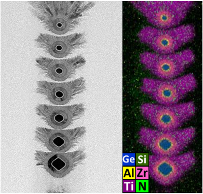
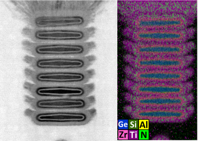
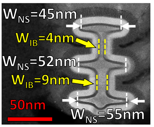
| Scientific Breakthrough | "This project successfully fabricated the world's first high-efficiency 7 stack GeSi nanowire. Compared with international benchmarks, its driving current achieves the world record for Ge/GeSi 3D transistors. The floor number of our 8 stack GeSi nanosheets exceeds that of French semiconductors research institute, CEA-Leti, published seven-layer stacked Si nanosheets in 2020. After understanding the factors that affect the performance of the device, our group is then integratedmatched with EPI technology, S/D contact technology, etching technology, thermal annealing technology, gate stack technology, transistor structure designprocess integration development,established scalingstacking of GAAFET for HMCSPICE model |
||
| Industrial Applicability | TSMC has used the high mobility channel (HMC) in the 5nm node. The HMC operates like a sports car that achieves the high speed with high horsepower, yielding a high-performance transistor. Samsung (3nm), Intel (2nm),TSMC (2nm) take advantage of the GAA transistor structure for advanced technology nodes. The GAA structure is like a powerful, no-leak faucet, which provides the transistor with low leakage current to save energy. The GAA structure with channel stacking provides large drive current for a given footprint to achieve high performancearea scaling. Consequently, the highly stacked (≥7) GAA transistor with HMC is the key for advanced nodes. |
||
| Keyword | Ge Epitaxy Growth S/D Regrowth Stacked GAAFETs NCFETs Atomic Layer Technologies Lithography Memristor Self-heating Effect PPAC(Power, Performance, Area, Cost) | ||
- Contact
- Chee Wee Liu
- cliu@ntu.edu.tw
other people also saw