


| Technical Name | 高質化石墨烯晶圓於下世代半導體之磊晶應用 | ||
|---|---|---|---|
| Project Operator | National Central University | ||
| Project Host | 蘇清源 | ||
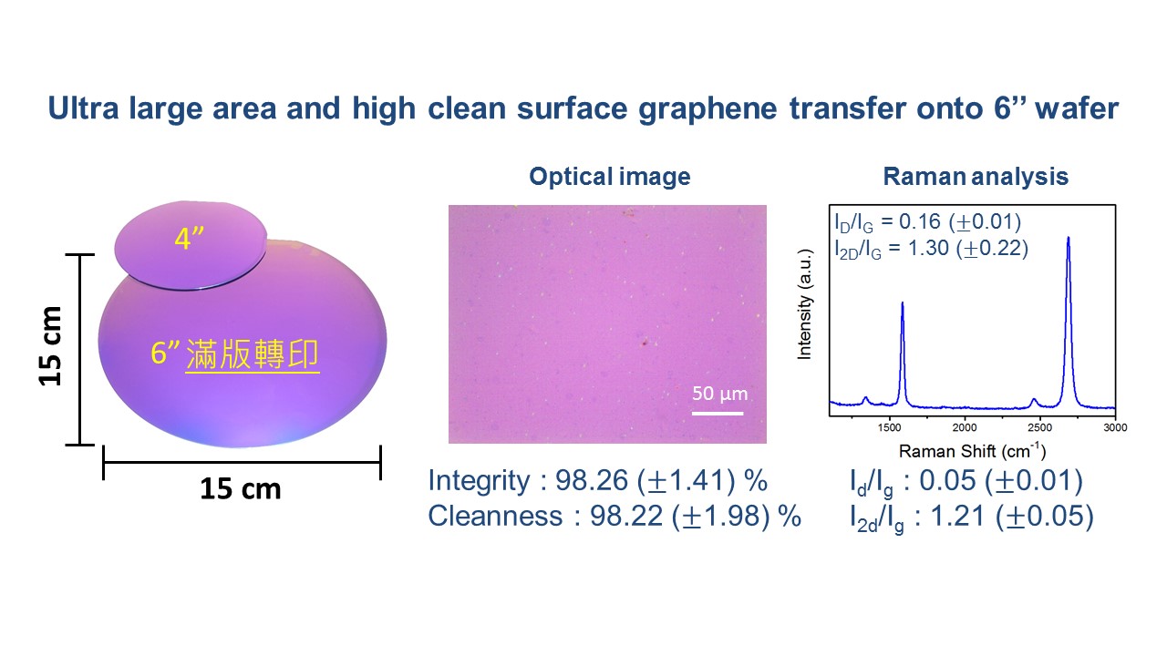
| Summary | In this technique, it can synthesize high-qualitylarge area graphene. We develop batch to batch chemical vapor deposition (B2B-CVD) to reduce the cost to facilitate the industrialized production. At the same time, the development of high-quality six-inch graphene silicon wafers was made with our unique transferring process. The wafer can be used as epitaxial substrates, which can solve the bottleneck of poor heat dissipation of sapphire substrates, lattice mismatch of Si substrates,expensive SiCGaN substrates. |
||
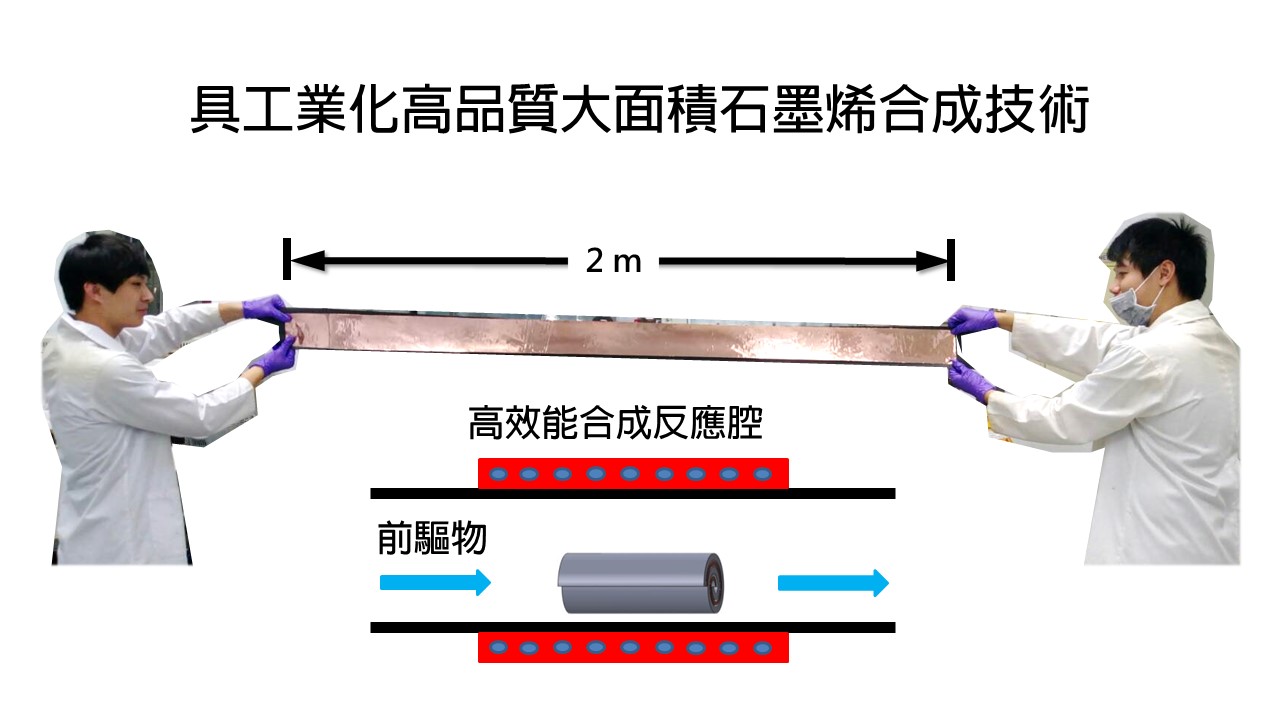
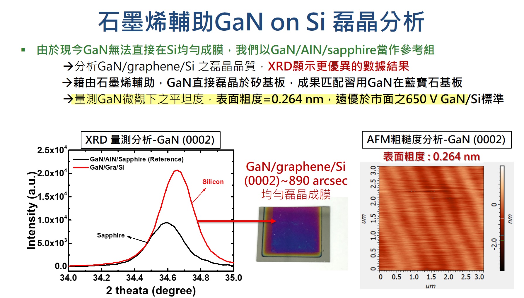
| Scientific Breakthrough | 1. Use economical equipment integrated our patented high-density rolling method to achieve scale up synthesis of high qualitylarge-area graphene for industrialized production. When the reaction chamber diameter reaches 8 inches, the productivity can be increased to 6.7 m2/h, which can reduce the cost. 2. Ultra-high clean transfer printing process, so that the surface cleanliness meets the specifications for making electronic components. 3. The GaN epitaxy process is performed on graphene as the buffer layer on the Si substrate to obtain high-quality crystalline state. |
||
| Industrial Applicability | The lattice structure of graphene has a good match with that of GaN,it can be applied to epitaxial fabrication process. If high-quality graphene is transferred onto a silicon wafer for epitaxy, which can replace the conventional sapphire substrate for epitaxy. That can solve the bottlenecks of poor heat dissipation, lattice mismatch,expensive SiCGaN substrates encountered by conventional sapphire substrates. It can produce high-efficiencycost-economic niche components, such as high-power/high-frequency electronic components, microwave components, short-wavelength LED/Laser. |
||
| Matching Needs | 天使投資人、策略合作夥伴 |
||
| Keyword | graphene semiconductor epitaxy substrate high power device | ||
- cysu@ncu.edu.tw
other people also saw