


| Technical Name | Industrialized synthesis technique of high quality and ultra-large area graphene | ||
|---|---|---|---|
| Project Operator | National Central University | ||
| Project Host | 蘇清源 | ||
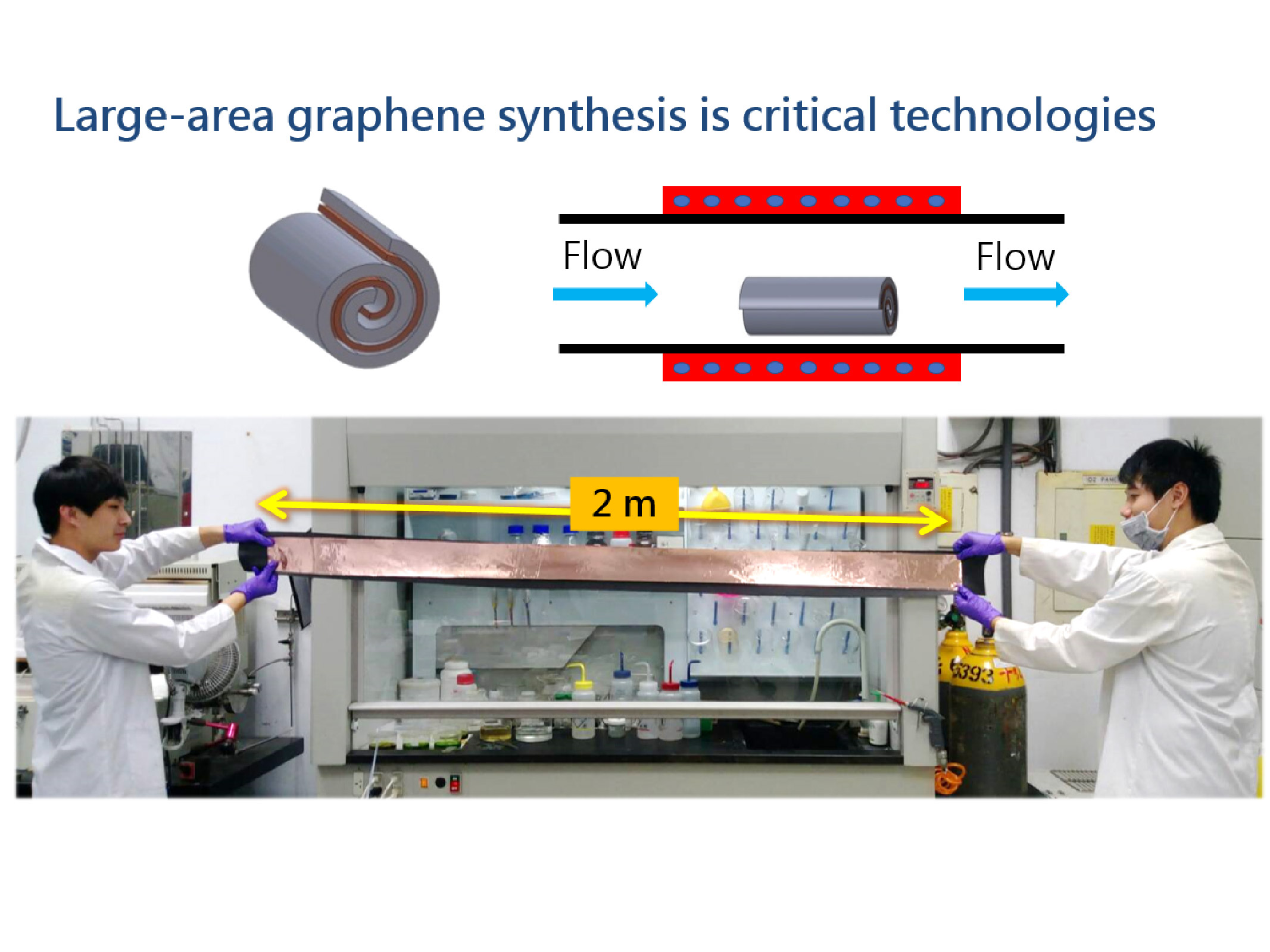
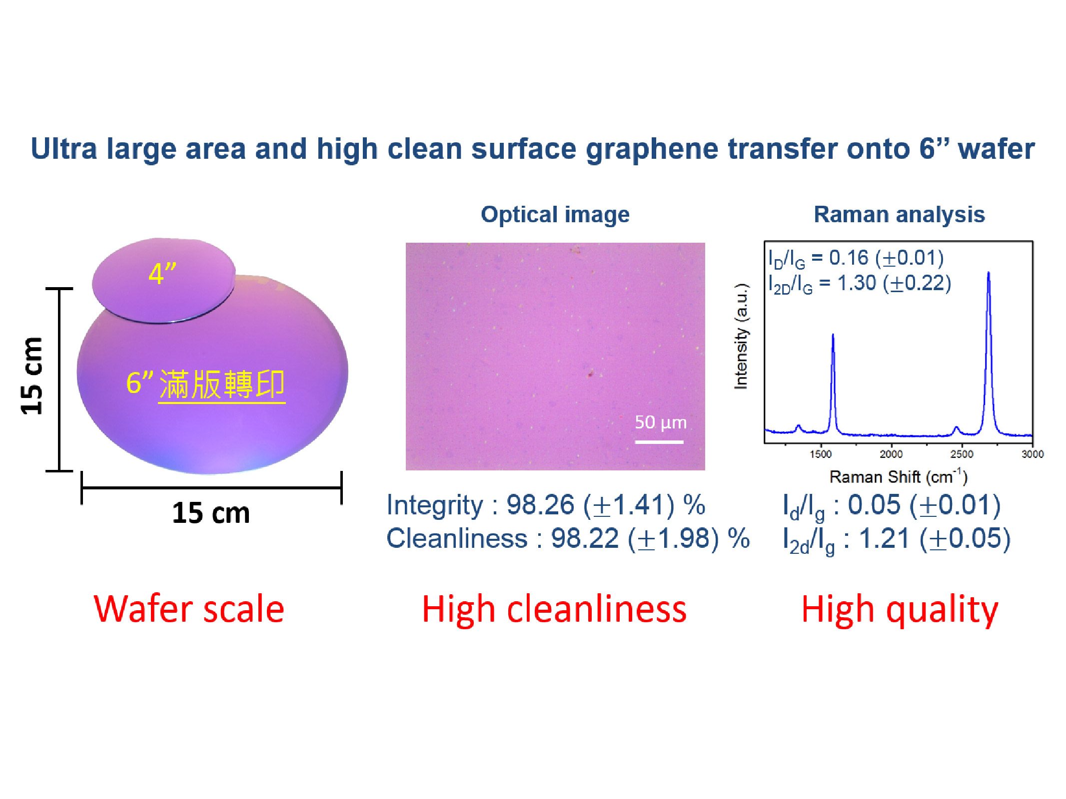
| Summary | In this technique, we develop batch to batch chemical vapor deposition (B2B-CVD) to reduce the cost to facilitate the industrialized production. In R2RCVD, in order to grow large-scale graphene in economic furnace tube, rolling the copper foil combined with quartz scaffold and isolated layer to overcome the problem of copper foil adhesion in high temperature. Furthermore, the optimized condition of gas flow rate, temperature, distance, and time have been found. By adopting our technique, a large-area graphene with an area of 5×100 cm2 can be obtained, domain size about 20 μm, sheet resistance only 750 Ω / sq, ID/IG radio 0.3, I2D/IG radio 0.9, defect density 2.43×1012 cm-2,and its charge carrier mobility ~1000 cm2V-1s-1. This invention can produce ultra large graphene with high-quality. It adopts simple operation and economic reaction components to increase the output of batch production of graphene to meet the needs of industrialization and marketization. |
||
| Scientific Breakthrough | The equipment of roll-to-roll technology for growing large-area graphene developed by Samsung or Sony is expensive and the control of parameters must be very precise. |
||
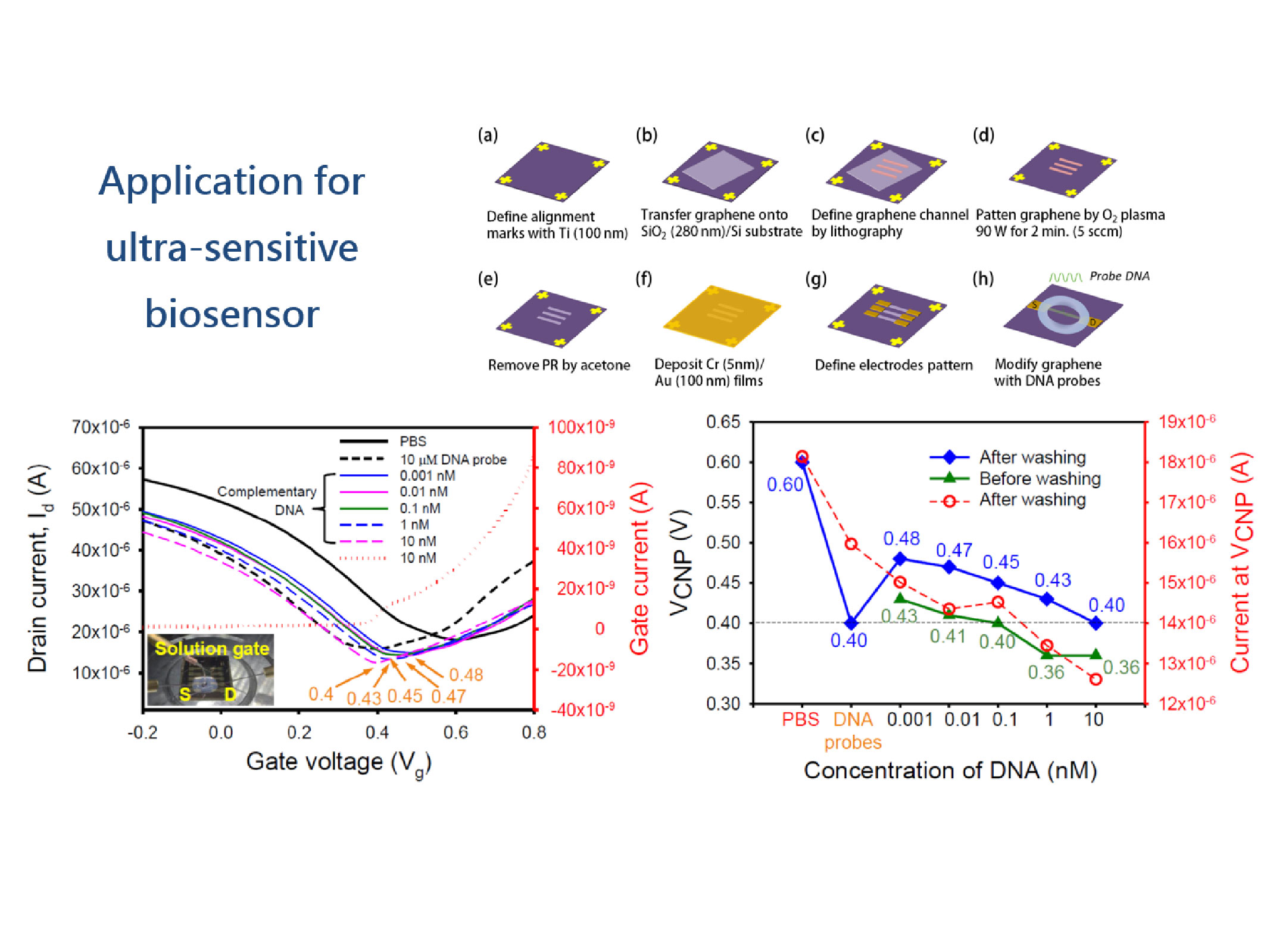
| Industrial Applicability | 1. Graphene has high light transmittance (light transmittance of single-layer graphene is 97%), high thermal and electrical conductivity and flexibility, which is suitable for ultra-high transparent conductive film. |
||
| Keyword | Graphene large area synthesis conductive film transistor biochip sensor epitaxial GaN 5G LED | ||
- cysu@ncu.edu.tw
other people also saw