


| Technical Name | Low-Temperature Defects Elimination Technology for Semiconductor devices | ||
|---|---|---|---|
| Project Operator | National Sun Yat-sen University | ||
| Project Host | 張鼎張 | ||
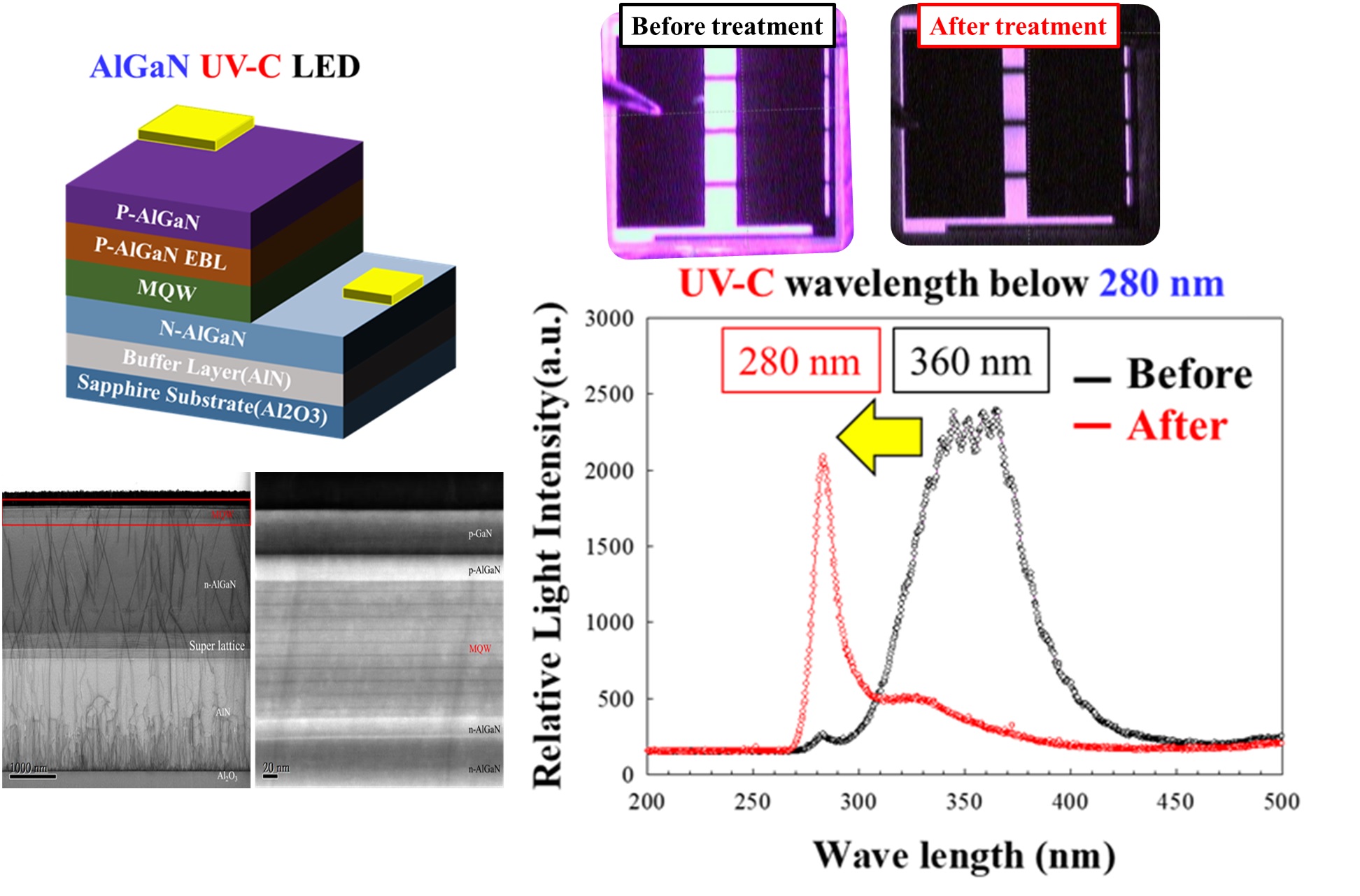
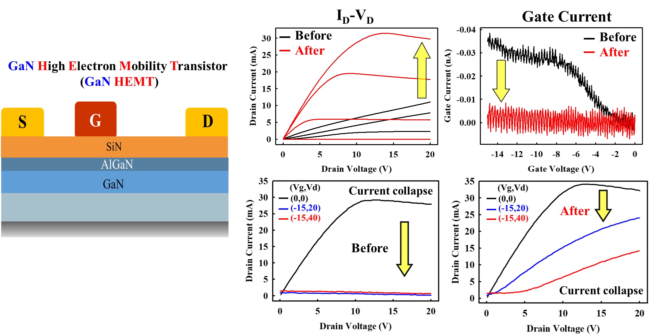
| Summary | The low-temperature defect passivation technology developed by our team can effectively eliminate defects in materials under 250°C, and leads to the improvement of the performance and reliability of devices. The technology has demonstrated the significant performance improvement when applying on GaN-based devices. After the treatment, the conducting current of FET devices is increased with the same operation condition. Moreover, in terms of LED devices, the emission efficiency was enhanced and the forward operating voltage decreased as well. |
||
| Scientific Breakthrough | The low-temperature defect elimination technology has novel principles. We can introduce specific reactant into semiconductor materials, and significantly passivate material defects with this technology. Then the performance and reliability of semiconductor devices are both improved. The technological breakthrough lies in the effective elimination of defects at low temperatures (250°C). We provide a new manufacture method of defect elimination, in addition to high temperature annealing and plasma. |
||
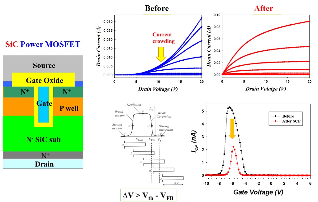
| Industrial Applicability | This technology has many potential applications, including Si devices and wide band gap semiconductors (LED, GaN HEMT, SiC MOSFET). It can be introduced into both the front and back end process of IC manufacture due to the low temperature. |
||
| Matching Needs | - |
||
| Keyword | Low-Temperature Defects Elimination Technology Low-Temperature process Back end of line, BEOL wide bandgap semiconductor material defects performance and reliability of semiconductor devic Si MOSFET LED GaN HEMT SiC MOSFET | ||
- iro926@gmail.com
other people also saw