


| Technical Name | Interlaced coupling layout for a doubly-parallel-coupled dual-band BPF | ||
|---|---|---|---|
| Project Operator | National Changhua University of Education | ||
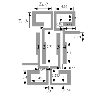
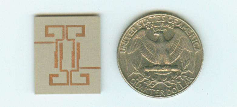
| Summary | The dual-band bandpass filter (BPFs) based on the doubly parallel-coupled stepped impedance resonators (SIRs) structures were proposed in this document. The proposed filter has the advantages of a much wider bandwidth in both the passbands without sacrificing the passband’s insertion loss and passband flatness. The interlaced circuit layout for the doubly-parallel-coupled SIR filter design allow this circuit to have multiple transmission zeros which are used to enhance the filter’s signal selectivity and the stopband performance. |
||
| Scientific Breakthrough | The dual-band bandpass filter (BPFs) based on the doubly parallel-coupled stepped impedance resonators (SIRs) structures were proposed in this document. The coupled-SIRs with open-stub-loads were introduced in the filter design. The dual-band filters exhibiting multiple zeros design operate at 2.45/5.5 GHz for the WLAN applications. Two three-staged filters composed of four SIRs were proposed with the tapped-line adapted in the I/O sections. The proposed filter has the advantages of a much wider bandwidth in both the passbands without sacrificing the passband’s insertion loss and passband flatness. The design procedure for a conventional parallel-coupled microstrip lines model is still suitable to design the proposed filters. The interlaced circuit layout for the doubly-parallel-coupled SIR filter design allow this circuit to have multiple transmission zeros which are used to enhance the filter’s signal selectivity and the stopband performance. Also the interlaced coupling structure of this filter design provides a compact circuit layout to save the circuit size. The fabrication of this circuit is based on the printed circuit board technology which allows itself to be built by a very low cost and to be massive produced without any difficulty. The PCB technology also grants the circuit the advantages of low cost, low profile, easy of mass production. In conclusion, we have the following: |
||
| Industrial Applicability | 需要無線通訊或是無線傳送與接收的場合越來越多,未來市場可期。 |
||
other people also saw