


| Technical Name | In-situ Monitored Thin Film Coating System and Process | ||
|---|---|---|---|
| Project Operator | National Applied Research Laboratories | ||
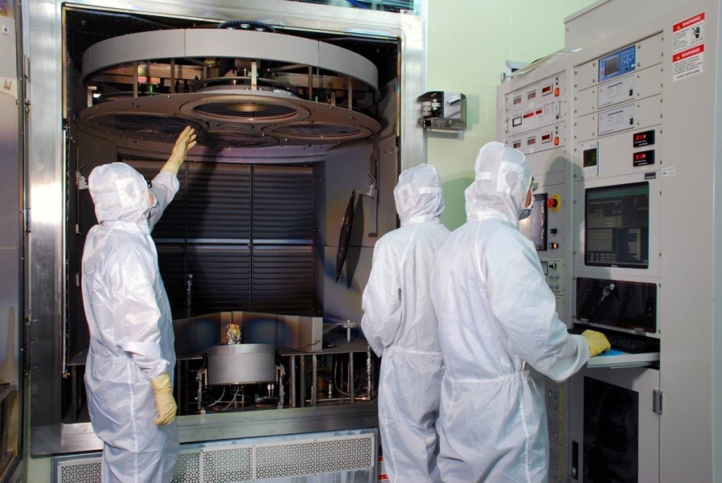
| Summary | Angstrom-scale surface roughness ion beam assisted deposition (IBAD) metal films were fabricated by in-situ optical monitored ion figuring. The surface roughness was characterized by AFM and XRR analysis. |
||
| Scientific Breakthrough | Angstrom-scale surface roughness ion beam assisted deposition (IBAD) metal films were fabricated by in-situ optical monitored ion figuring. The surface roughness was characterized by AFM and XRR analysis. It was found that the root-mean-square (RMS) surface roughness has been improved from above 6 nm for an as coated IBAD Au film to 0.462 nm for the in-situ optical monitored ion figuring treated IBAD Au film, respectively. By the same way, in-situ ion figured extreme smooth IBAD Ag film with 0.124 nm (RMS) was measured by AFM. Furthermore, films are characterized by a significantly lower RMS surface roughness and narrower peak-to-valley surface topological height distribution. The present invention provides the essential technology of 13.5 nm extreme ultraviolet optical components for the next generation photolithography technology of domestic semiconductor industries. In the development of 2D materials, this technology provides uniform and extreme smooth front-end process. Therefore, the present invention fulfills the critical needs among national scientific missions, development of industries and new materials. |
||
| Industrial Applicability | 本技術除光學元件與鍍膜產業之外、對先進同步輻射 (台灣光子源) 科學儀器之光學元件所需極平整表面鍍膜技術亦可提供國內自製之技術支援能力;對我國半導體下世代半導體曝光技術 (photolithography) 亦可提供 13.5 nm 極紫外光學元件之薄膜製鍍關鍵技術,以降低產業整體資本門支出並提升設備在地化之基礎工業能力;在先進二維材料之發展上亦可提供均勻且平整之前段製程,故本項發明專利於國家科學任務、產業發展與新材料之開發等方面均極具重要性。 |
||
other people also saw