


| Technical Name | Technology for the system packaging of medical detection chip in the silicon photon technology | ||
|---|---|---|---|
| Project Operator | National Central University | ||
| Project Host | 李天錫 | ||
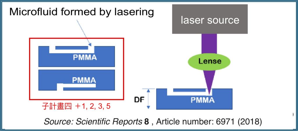
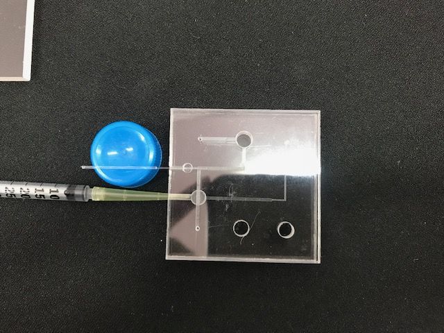
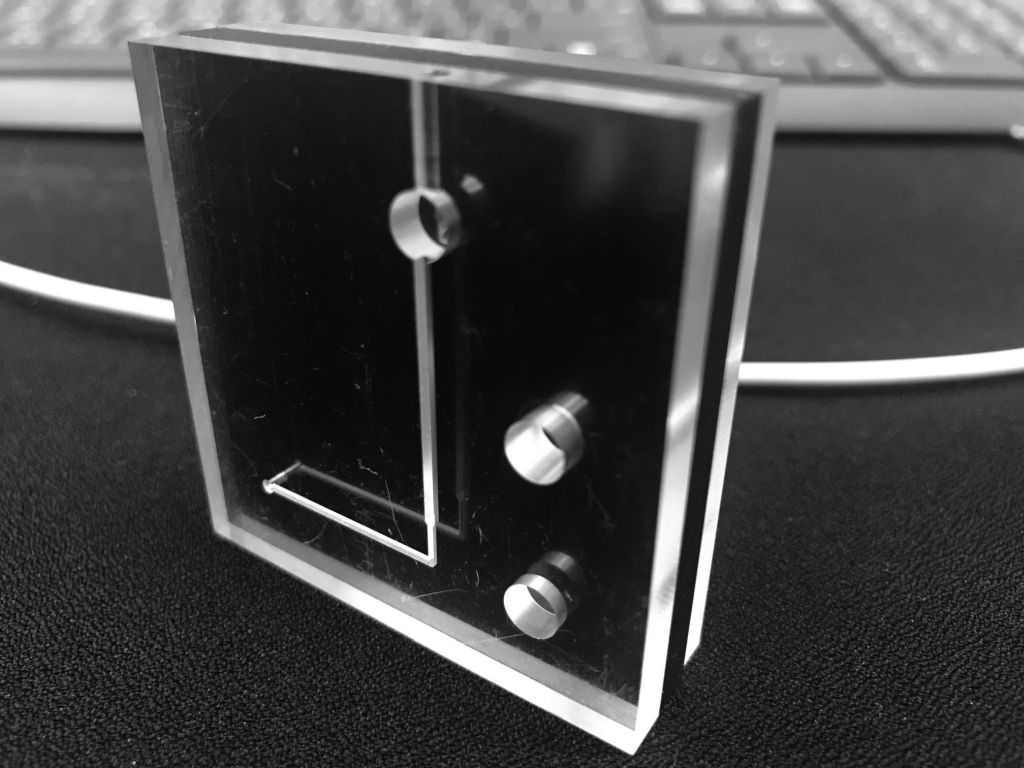
| Summary | The wafer bonding technology and laser processing technology are combined to form a stereo microchannel biomedical test wafer. The wafer device can simultaneously accept and detect the same blood sample by Raman and OCT detection sensors to achieve the highest purpose in accurancy. The device will also reconcile the AI, Artificial Intelligence, and the big data analysis technologies to achieve a high speed biomedical test chip. |
||
| Scientific Breakthrough | First, break through the conventional microfluidic design by a 3D design to integrate OCT and Raman spectroscopy into one evaluation. Second, break through the limitations of the optical properties of materials to directly engrave microchannels by lasing. Third, break through the material temperature limit by using low-temperature wafer bonding technology to maintain high accuracy specifications. |
||
| Industrial Applicability | This biomedical testing chip is mainly used in the medical equipment market, and can also be extended to the pharmaceutical, chemical and food testing industries. This The microfluid chip is expected to replace the traditional for drawing the amount of blood to half-needle. It requires only takes tens of seconds for Raman and OCT interactive detection to obtain perfect detection results. |
||
| Keyword | Low temperature wafer bonding Stereo microfluids Laser processing Raman spectroscopy OCT images PMMA Micro-processing Biomedical chip Clotting factor Fabrication on First Come First Served Silicon photonic component | ||
- t1995tony@gmail.com
other people also saw