


| Technical Name | A method of Cryo-electrochemistry to Fabricate Nanocrystals on Si Substrate | ||
|---|---|---|---|
| Project Operator | National Central University | ||
| Project Host | 李天錫 | ||
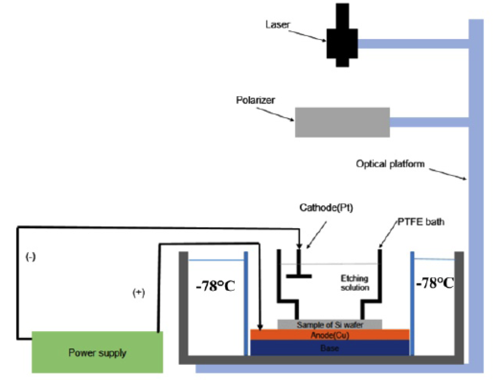
| Summary | The technology uses an electrochemical etching technique to produce a high dense, uniform, single crystal orientation nanocrystalline process. The etch tank can be stored in a -78 ° C dry icealcohol mixed cooling medium, with the ability to cool down to -20 ° C, maintain a constant temperature for electrochemical etching, forming 4-5 nm nanocrystal. |
||
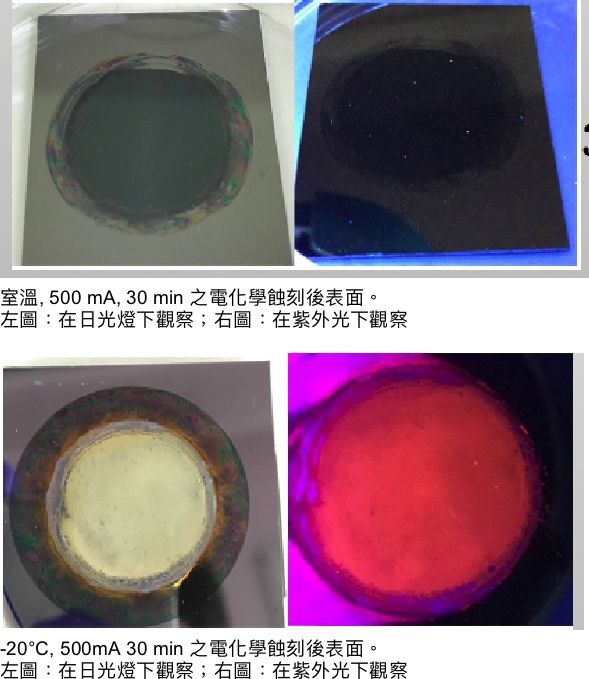
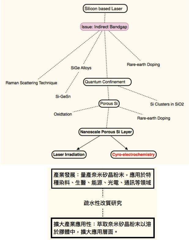
| Scientific Breakthrough | Under the same electrochemical conditions, the photoluminescence effect of the p++ type porous silicon produced at room temperatureunder cryogenic conditions is quite different. The nanocrystal size of silicon obtained at normal temperature is about 15 nm,the nanocrystal size obtained under deep cooling is 5 nm,the size reduction ratio is 300, that is very remarkable. |
||
| Industrial Applicability | The technology can effectively produce nano crystals,make nano crystal coatings in solution, which are applied in different productstechnologies, such as anti-counterfeiting devices. In addition to its application in the photon, it has great potential in the biomedical industry, for example, it can be used as a fluorescent substance to find cancer cells. |
||
| Keyword | Nanocrystals Cyro-electrochemistry Crystalline silicon Biophotonic applications Silicon photonics Quantum Confinement Flash memory Optoelectronic Applications Microphotonics silicon Photovoltaic applications | ||
- Jpbgji4@yahoo.com.tw
other people also saw