


| Technical Name | Semiconductor device structuremethod for forming the same | ||
|---|---|---|---|
| Project Operator | National Taiwan University | ||
| Project Host | - | ||
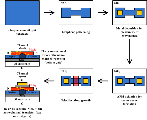
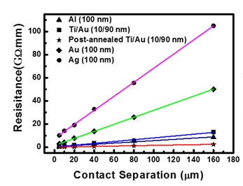
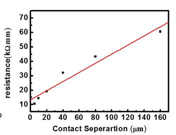
| Summary | With (a) the good device performances of MoS2 transistors with short channel lengths, (b) the low contact resistance of graphene on MoS2(c) the epitaxially grown graphene/MoS2 hetero-structures, we proposed a MoS2 transistor architecture fabricated by using AFM anode oxidation on graphene/MoS2 hetero-structures. With additional gate dielectric layer deposition, both bottom-top- gate devi |
||
| Scientific Breakthrough | - |
||
| Industrial Applicability | - |
||
| Keyword | __- | ||
- futuretech.most@gmail.com
other people also saw