


| Technical Name | Negative capacitance field effect transistor with charged dielectric material | ||
|---|---|---|---|
| Project Operator | National Taiwan University | ||
| Project Host | 李嗣涔 | ||
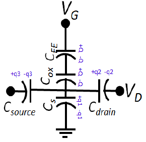
| Summary | The present disclosure provides a semiconductor device in accordance with some embodiments. The semiconductor device includes a substrate a gate stack over the substrate. The gate stack includes a ferroelectric layer a first dielectric material layera first conductive layer. One of the first dielectric material layerthe ferroelectric layer is electrically charged to form a charged lay |
||
| Scientific Breakthrough | - |
||
| Industrial Applicability | - |
||
| Keyword | |||
- futuretech.most@gmail.com
other people also saw