


| Technical Name | Highly stacked channels with extremely high-k gate stacks Stacked nanosheet FeFET IGZO GAA nanosheet | ||
|---|---|---|---|
| Project Operator | Graduate Institute of Electronics Engineering, National Taiwan University | ||
| Project Host | 劉致為 | ||
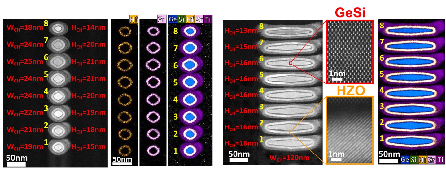
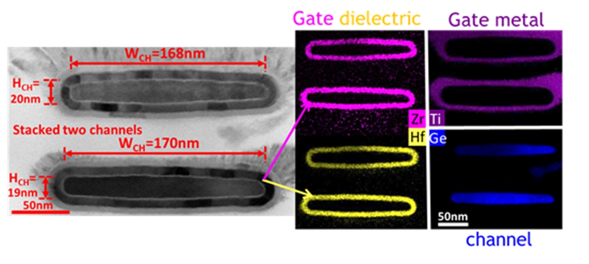
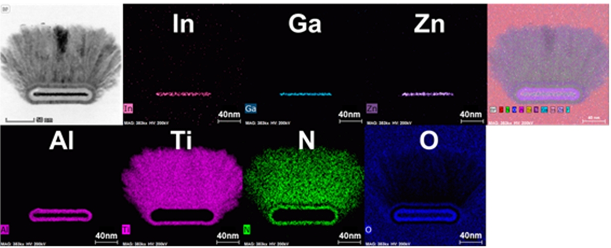
| Summary | Highly stacked channels are with extremely high-k gate stacks. The nanowiresnanosheets achieve record ION per footprint (9200μA/μm)record ION per stack (360μA) at VOV=VDS=0.5V, respectively The stacked GeSi nanosheet FeFETs feature large memory window of 1.8V at low write voltage of 2V, stable storage with data retention of 1E4 seconds,high endurance 1E11 cycles The a-IGZO GAA Nanosheet features SS of 61mV/dec, Ioff1E-7uA/um, DIBL of 44mV/V,positive threshold voltage. |
||
| Scientific Breakthrough | The extremely high-k Hf0.2Zr0.8O2 gate stacks, 8 stacked channels,high mobility Ge0.95Si0.05 channels are all integrated to achieve the record ION First stacked GeSi nanosheet GAA FeFETs. Our work with the large memory window of 1.8V at the low write voltage of 2V, high MW/VP/E ratio of 0.45,stacked GeSi nanosheets structure lead the world First a-IGZO GAA Nanosheet FET. The SS of 61mV/dec, positive VT, leakage current 1E-7 μA/μm,GAA nanosheet structure lead the world. |
||
| Industrial Applicability | To extend lifetime of stacked nanosheets, the high mobility channels, highly stacked channels,extremely high-k are used to further improve device performance. It is expected to be used beyond 2nm technology node FeFETs are promising candidates for embedded non-volatile memory with CMOS-compatible process for scalability. The large MW at the low write voltage can be obtained The a-IGZO GAA Nanosheet FET can be used in applications of monolithic 3D, 2T0C DRAM, FeFET,compute-in-memory. |
||
| Keyword | Extremely high-k gate dielectrics Highly stacked channels High mobility channel Stacked nanosheet FeFETs FeFET Non-Volatile Memory Memory window Endurance Amorphous InGaZnO (a-IGZO) GAA nanosheet FET | ||
- Contact
- Chee Wee Liu
- cliu@ntu.edu.tw
other people also saw