


| Technical Name | Beyond Silicon: Advanced Two-Dimensional Semiconductor Transistor Technologies | ||
|---|---|---|---|
| Project Operator | National Yang Ming Chiao Tung University | ||
| Project Host | 簡紋濱 | ||
| Summary | For the applications of two-dimensional (2D) semiconductors in future semiconductor technologies, several essential bottleneck problems are resolved. We develop an ion-bombardmentthermal annealing for repairing defects on surface of 2D semiconductors (such as PdTe2PtTe2), a high-speed switching of field-effect transistors (FETs) with ultrathin high-k Ta2O5 dielectrics, an extremely low-resistance contact technique with grapheneTaS2, low-temperature (250oC) epitaxy of h-AlN as dielectrics for gate-all-around field-effect transistors,low-temperature (600oC) wafer-scale epitaxy of crystalline 2D semiconductors (WS2). These key advances push 2D semiconductors approaching feasible applications in future electronics. |
||
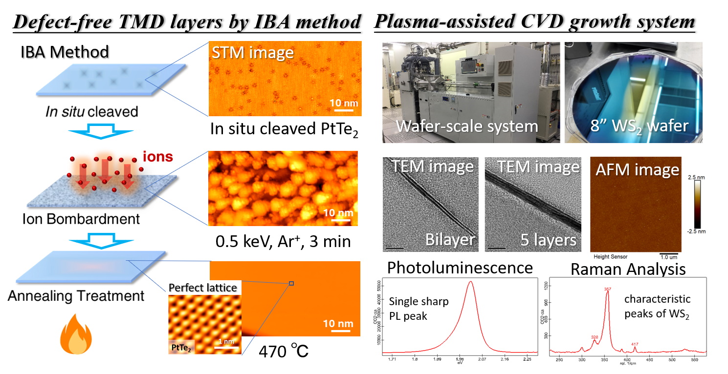
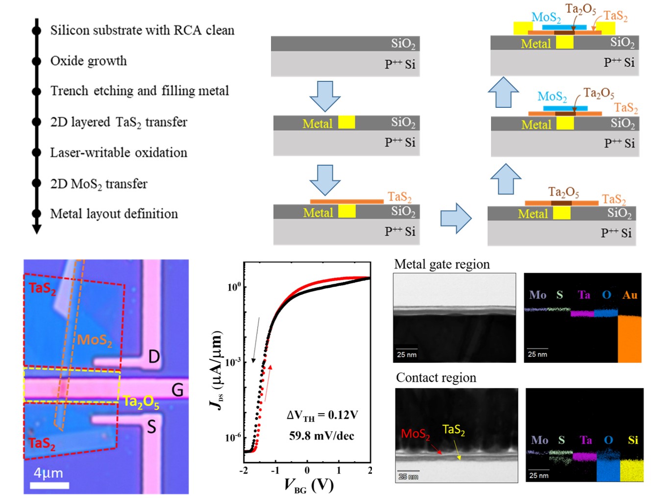
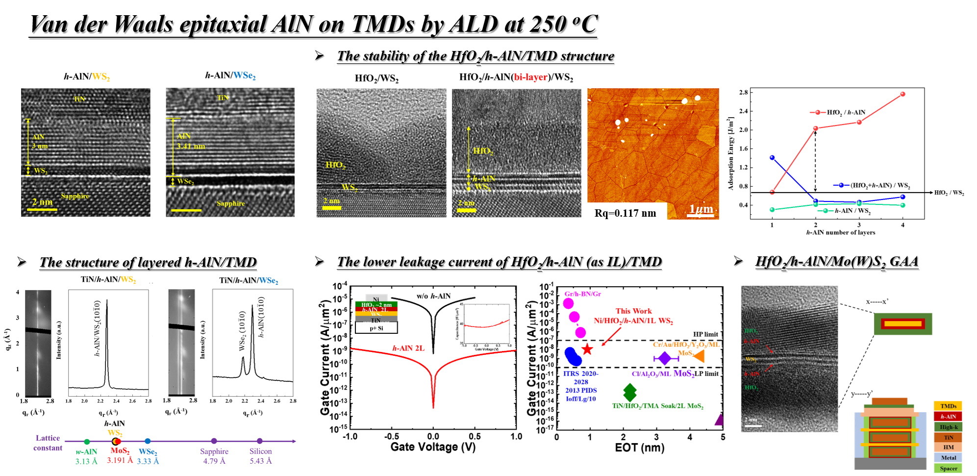
| Scientific Breakthrough | 2D semiconductors show reduced short-channel effects, high on-off ratiohigh mobilities. However, it is difficult in film epitaxyvulnerable to semiconductor processing. We implement interfacial science to solve the difficulties. We employ oxidation of TaS2 to form Ta2O5 layers as dielectricsatomic-layer deposition to insert h-AlN layers. With this interface, the 2D semiconductors are protected while the device performances are promoted to reveal the lowest subthreshold swing of 59.8 mV/dec. The contact resistance is reduced to 50 Ω·μm. We employ ion bombardmentthermal annealing to heal surfacereduce surface defects down to 10^10 cm-2. These technologies are uniquecan overcome the current technical bottleneck. |
||
| Industrial Applicability | Two-dimensional semiconductors show promising applications to high-densityhigh-performance transistor technologies, such as gate-all-around (GAA)monolithic 3D-IC, beyond the 2 nm technology node. Our center develops advancednovel 2D semiconductor technologies, including ultrathinhigh-k Ta2O5h-AlN interface layers, extremely low-resistance contact technology, ion-bombardmentannealing of surface repairing technology,large-scale epitaxy, breaking through the technical bottlenecks for the application of the next-generation semiconductor industry. With these technologies, it can sustain the leading role of Taiwan's semiconductor industrycreate opportunities of trillion-dollar business. |
||
| Keyword | two-dimensional semiconductor wafer-scale growth ultra-thin Ta2O5 dielectrics ultralow contact resistance ion bombardment surface defects h-AlN epitaxy | ||
- Contact
- Yen-Teng Ho
- chia500@nctu.edu.tw
other people also saw