


| Technical Name | Development for Advanced High-Density Monolithic Three Dimensional Integrated Circuits with Multi-stacked Transistor Layers | ||
|---|---|---|---|
| Project Operator | Department of Photonics, National Yang Ming Chiao Tung University | ||
| Project Host | 劉柏村 | ||
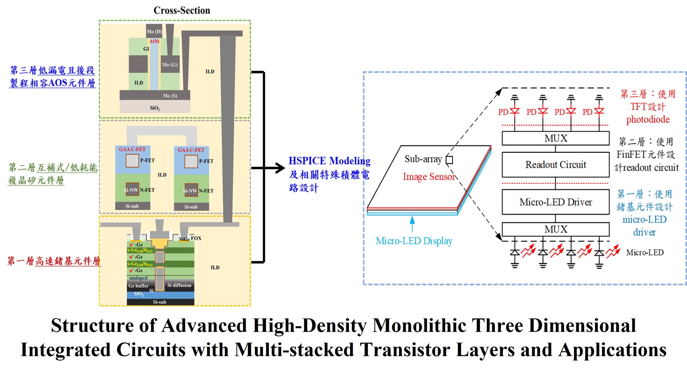
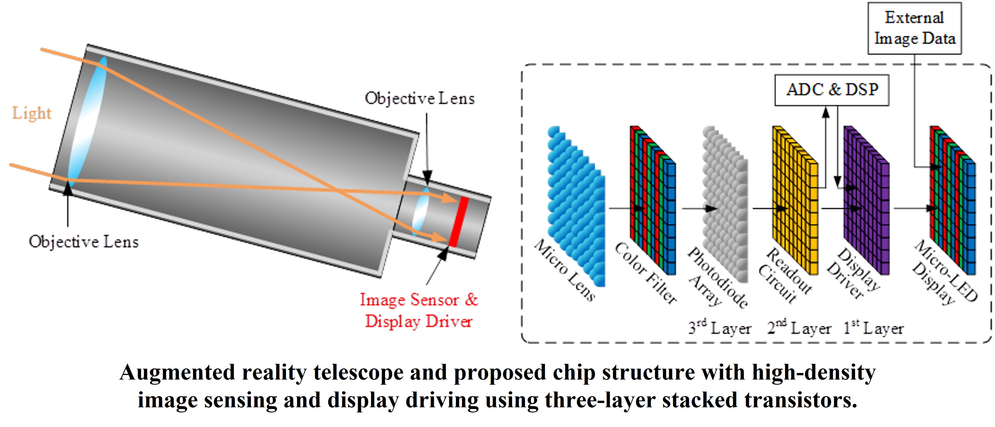
| Summary | The aim of this project is to develop Advanced High-Density Monolithic Three Dimensional Integrated Circuits with Multi-stacked Transistor Layers by integrating three layers of high-performance stacked transistorsextending them to the circuit design of application-specific integrated circuits (ASICs). The research contents include the developments of novel semiconductor materials, high-performance GAAFET devices, the device model establishment,circuit designs for ASICs. Based on the device models of three-layer stacked transistors, the driver IC design of augmented reality telescopes with image sensorsmicro-LED display circuits is realized to demonstrate the technology feasibility of the proposed M3D-ICs. |
||
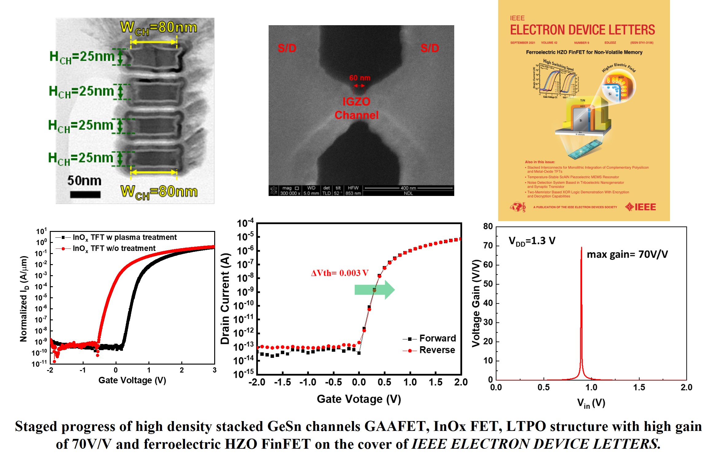
| Scientific Breakthrough | We have developed high-performance transistors for the Monolithic Three Dimensional Integrated Circuits (M3D-ICs). Also, the technology feasibility of three-layer stacked transistors have been investigated, showing high potential for high-density 3D-ICs. The GeSn p-channel GAAFET, Poly-Si FinFET with negative capacitor, Ferroelectric FinFET-based memory, high-performance InOx-based TFT have been achieved successfully. Based on these advanced transistors, device models will be establishedconstruct the high-density image sensordisplay driver circuits with shorten latency time from image sensing to display, demonstrating the potentialfeasibility of M3D-IC technology. |
||
| Industrial Applicability | High-mobility GeSn GAAFET, Poly-Si FinFETGAAFET with negative capacitance,high-performance indium oxide-based TFT have been successfully developed for monolithic 3D-IC integrationdemonstrated their technical feasibility. The device density of the advanced 3D-stacked transistors can reach 1.01 MTr/mm^2. Furthermore, the proposed 3D-stacked transistor architecture can be applied not only to the advanced semiconductor industry but also to ASICs technology, for example, for the implementation of driver ICs of augmented reality telescope applicable for national defense, marineastronomy. |
||
| Keyword | Monolithic Three Dimensional Integrated Circuits Amorphous Oxide Semiconductor Thin Film Transistor GeSn channel stacked Gate All Around Field Effect Ferroelectric Fin Field Effect Transistor Negative Capacitance Fin Field Effect Transistor Ferroelectric material Atomic Layer Deposition Application-specific Integrated Circuits Micro Light Emitting Diode Augmented Reality Telescope | ||
- Contact
- Tsung-Che Chiang
- tcchiang.ee08@nycu.edu.tw
other people also saw