


| Technical Name | 高解析度光學微影銀漿 | ||
|---|---|---|---|
| Project Operator | National Sun Yet-sen University | ||
| Project Host | 陳軍互 | ||
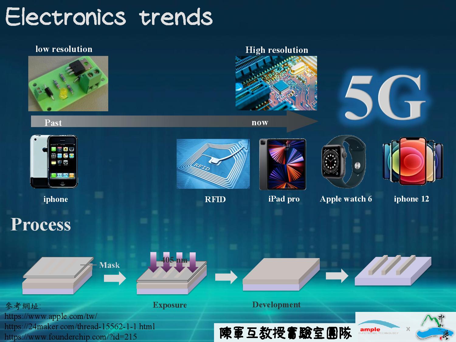
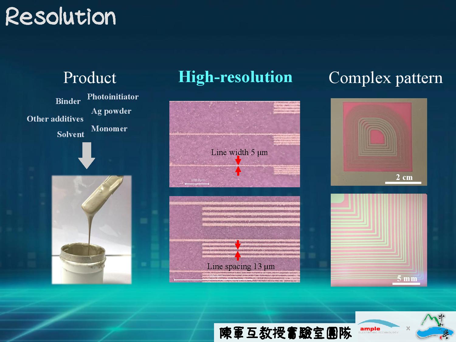
| Summary | Current 5G communication devices have a huge demand in high resolutiondensity of metal conducting wires in electronics ( 40 μm line width/line spacing), which cannot be achieved by conventional screen printing (100 μm). Our group cooperated with Ample Technology to develop a new-generation silver conductive paste which enables photolithographyachieves outstanding line resolution (5 μm width/13 μm spacing). The paste is simple to useperforms comparable of those of major European, AmericanJapanese manufacturers. |
||
| Scientific Breakthrough | Enhancing the adhesion of the circuit lines to the board after developing is an important aspect towards improving resolution by photolithography. The three factors to consider include (1) improvement of light absorption efficiency of the photosensitizer to increase polymerization degrees (2) controlled stability of free radicals to prevent expansion leading to short-circuiting of lines(3) reduced printing thickness for the higher light penetration efficiency. The factors above can influence the paste to achieve ultrahigh resolution by improving the adhesion of circuit lines. |
||
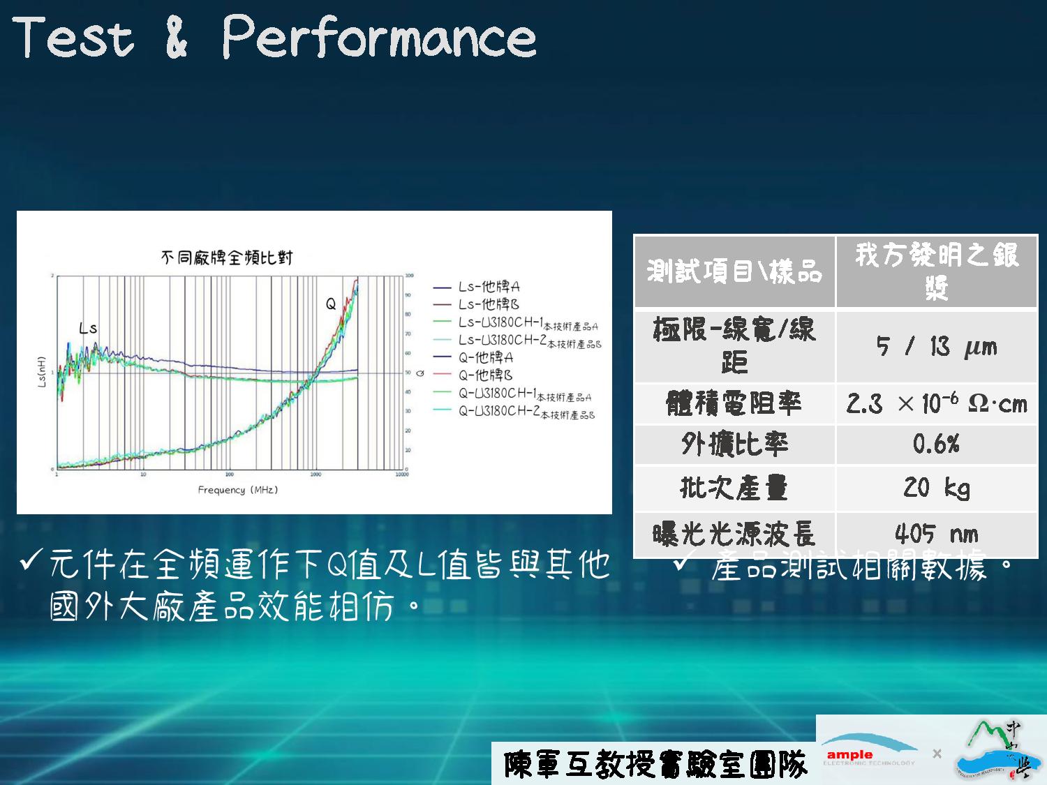
| Industrial Applicability | Mass production of the silver pastes is available (20 kg/batch). The simplified operation only needs three steps (printing, light exposure at 405 nm,developing) to produce high-resolution patterns with the optimal resolution (5 μm width/13 μm spacing). Silver conductive circuit (2.5*10-6 (Ω*cm) can be produced followed by the thermal sintering. The QL values of the device prepared by our pastes are similar to other international brands (see the attached figures).This product can be applied to all 5G related electronics required high resolution conductive wires. |
||
| Matching Needs | 天使投資人、策略合作夥伴 |
||
| Keyword | 5th generation wireless system 5G electronics photolithography paste high resolution silver screen printing Internet of Things circuit | ||
- chunhu.chen@mail.nsysu.edu.tw
other people also saw