


| Technical Name | 原子厚度的二維半導體元件 | ||
|---|---|---|---|
| Project Operator | National Synchrotron Radiation Research Center | ||
| Project Host | 陳家浩 | ||
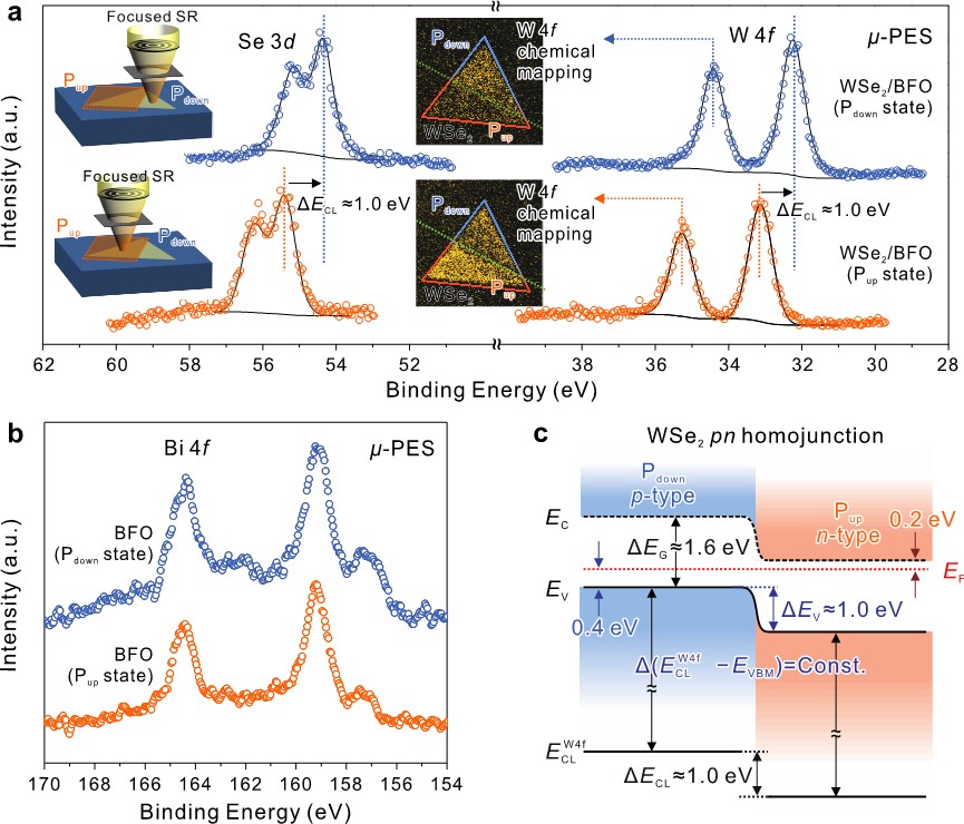
| Summary | We proposedshowed the ferroelectric materials served as a prospective substrate to support TMD to achieve a pn homojunction, as the accumulationdepletion of an inevitably charged mobile carrier occurs in the TMD to screen the polarization field of the FE substrate. This work provides a non-volatile control of TMD dopinga promising way to produce a pn homojunction as a future building block of 2D device applications. |
||
| Scientific Breakthrough | In recent years, the composite material made by combining materials have found ways to various applications including aviation, medicine, machinery,construction. In this study, we used a 2D composite material composed of a single-layer WSe2 semiconductorBiFeO3 to show that the electrical structure of the 2D material can be engineered without the addition of a metal electrode to achieve the effect of a diode. For the first time, it has been proved that the electronic structure of two-dimensional materials can be manipulated by the composite function of multiferroic materials. |
||
| Industrial Applicability | We proposedshowed the ferroelectric materials served as a prospective substrate to support TMD to achieve a pn homojunction, as the accumulationdepletion of an inevitably charged mobile carrier occurs in the TMD to screen the polarization field of the FE substrate. This work provides a non-volatile control of TMD dopinga promising way to produce a pn homojunction as a future building block of 2D device applications. |
||
| Matching Needs | 天使投資人、策略合作夥伴 |
||
| Keyword | 2D semiconductor 2D diode composite materials WSe2 BiFeO3 multiferroic 2D material superlattice electronic structure engineering quantum computer quantum material | ||
- chchen@nsrrc.org.tw
other people also saw