


| Technical Name | 2D material inspection technology | ||
|---|---|---|---|
| Project Operator | National Chung Cheng University | ||
| Project Host | 王祥辰 | ||
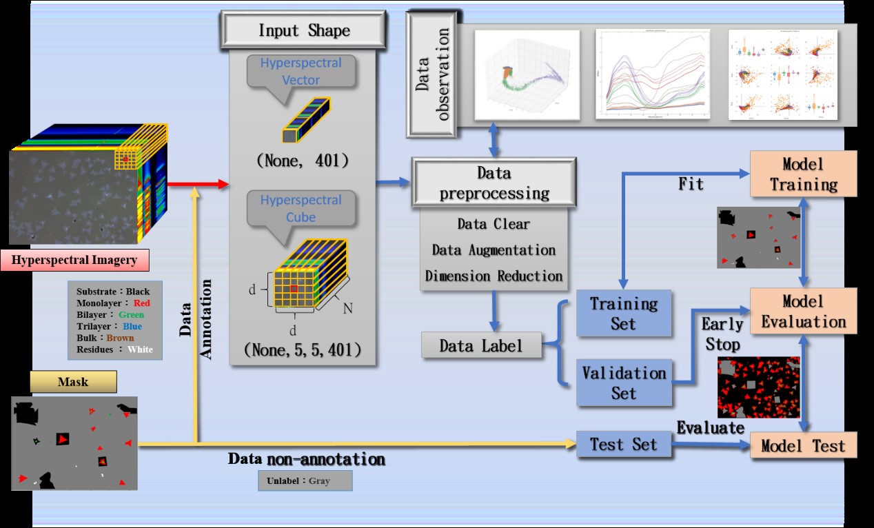
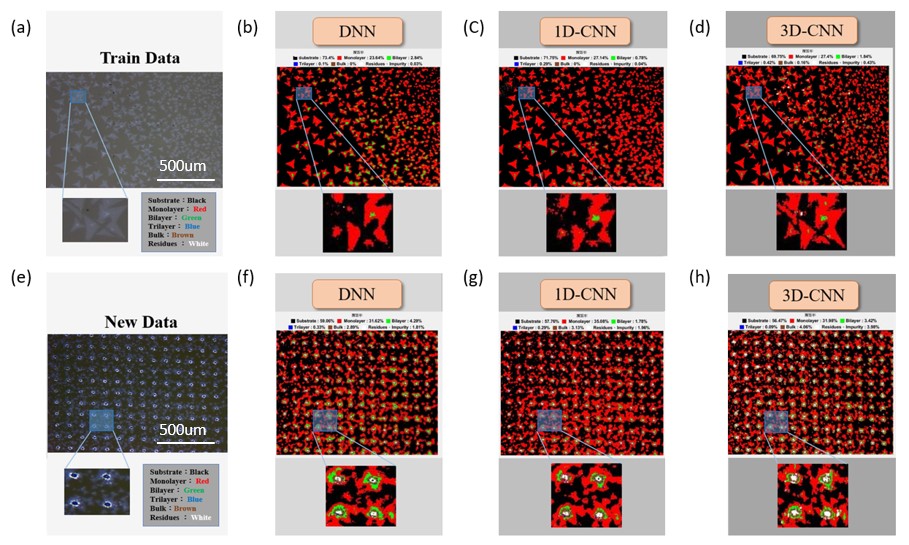
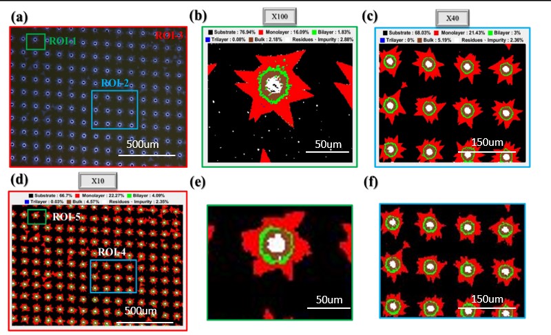
| Summary | We propose deep neural network, one-dimensional convolutional neural network, and three-dimensional (3D) convolutional neural network (3D-CNN) models to explore the correlation between the accuracy of model recognition and the optical characteristics of few-layers MoS2. The experimental results show that the 3D-CNN has better generalization capability than other classification models, and this model is applicable to the feature input of the spatial and spectral domains. Such a difference consists in previous versions of the present study without specific substrate, and images of different dynamic ranges on a section of the sample may be administered via the automatic shutter aperture. Therefore, adjusting the imaging quality under the same color contrast conditions is unnecessary, and the process of the conventional image is not used to achieve the maximum field of view recognition range of 1.92 mm2. The image resolution can reach 100 nm and the detection time is 3 min. per one image. |
||
| Scientific Breakthrough | A method for detecting a two-dimensional material is provided. In the method, a suitable OM image from a cloud database is converted into a space spectral data by a hyper spectral imaging technology of visible light and a Raman data of a grown layer number and a grown position of a sample are used as a label of data set, and the space spectral data and the label are used as an input of a model with 3D-CNN. |
||
| Industrial Applicability | With the superior performance of two-dimensional (2D) materials and its wafer-level synthesis methods, it has attracted more and more attention, aroused great interest and triggered a revolution in the application of corresponding devices. However, the large-scale characterization, accuracy, intelligent automation and high-efficiency detection of nanostructures for two-dimensional materials have not yet been successfully applied at industrial level. It can be applied to semiconductor industry, display, photoelectric material industry. |
||
| Keyword | hyperspectral imagery deep learning 3D-CNN 2d materials | ||
- hcwang@ccu.edu.tw
other people also saw