


| Technical Name | Investigations of probes for the applications in the high frequency and high speed IC testing system | ||
|---|---|---|---|
| Project Operator | Engineering & Technology Promotion Center | ||
| Project Host | 楊證富 | ||
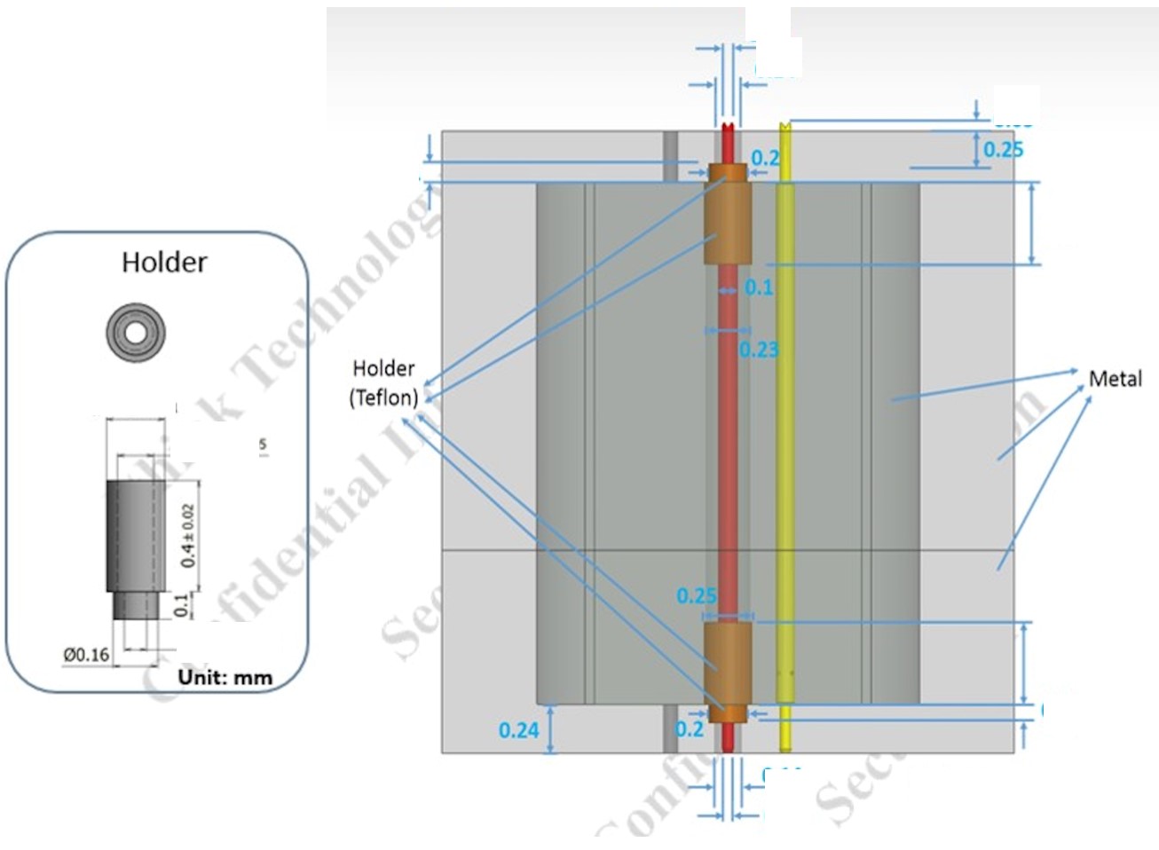
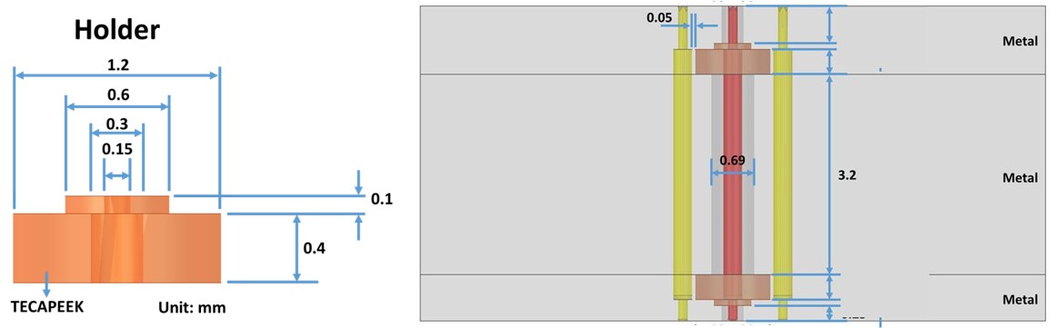
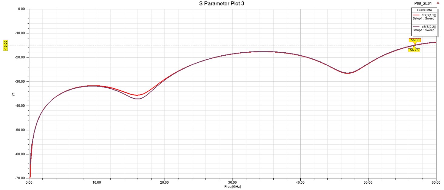
| Summary | At the first, we would design three different types of probes for high frequency and high speed IC testing system, including pitch 0.3mm, 0.4mm, and 0.8mm. Next, we use the Agilent’s Advanced Design System software to carry out the simulations of three different types of probes for high frequency and high speed IC testing system. Because the filling materials are used as the isolated layer, for that the simulations should use different filling materials, which have different dielectric constants. In this proposal, we use Teflon and epoxy to find the effect of the materials with the different dielectric constants on the properties of three different investigated probes. |
||
| Scientific Breakthrough | The tests of the semiconducting devices can be divided into the chip probe (CP, test before package) and final test (test after package). The wafer level chip scale package (WLCSP) is one kind of CP and it has the merit of reducing the package size, which can match the market development. This investigated technology is to 「investigate the probes for the applications in the high frequency and high speed IC testing system」. |
||
| Industrial Applicability | The tests of the semiconducting devices can be divided into the chip probe (CP, test before package) and final test (test after package). The wafer level chip scale package (WLCSP) is one kind of CP and it has the merit of reducing the package size, which can match the market development. This project is to 「investigate the probes for the applications in the high frequency and high speed IC testing system」. |
||
| Keyword | High frequency High speed; IC test system Probe Pitch Wafer level chip scale package (WLCSP) Scaling Fan-In WLP Fan-Out WLP Final test | ||
- cfyang@nuk.edu.tw
other people also saw