


| Technical Name | Hybrid CMOS Inverter Comprised of Thin Film Transistors with Hetero-channel for Monolithic 3D-ICs and Ultra-high Resolution Flat-Panel Displays Applications | ||
|---|---|---|---|
| Project Operator | Department of Photonics, National Chiao Tung University | ||
| Project Host | 劉柏村 | ||
| Summary | To overcome the physical limit in the device scaling, the monolithic 3D-IC technology with back-end-of-line process compability (<400 ˚C ) has received a lot of attention and been studied to replace typical 2D-IC circuit layouts. It can effectively increase circuit integration density in a single wafer and further reduce power consumption. |
||
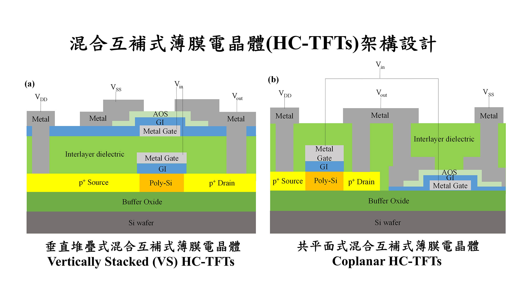
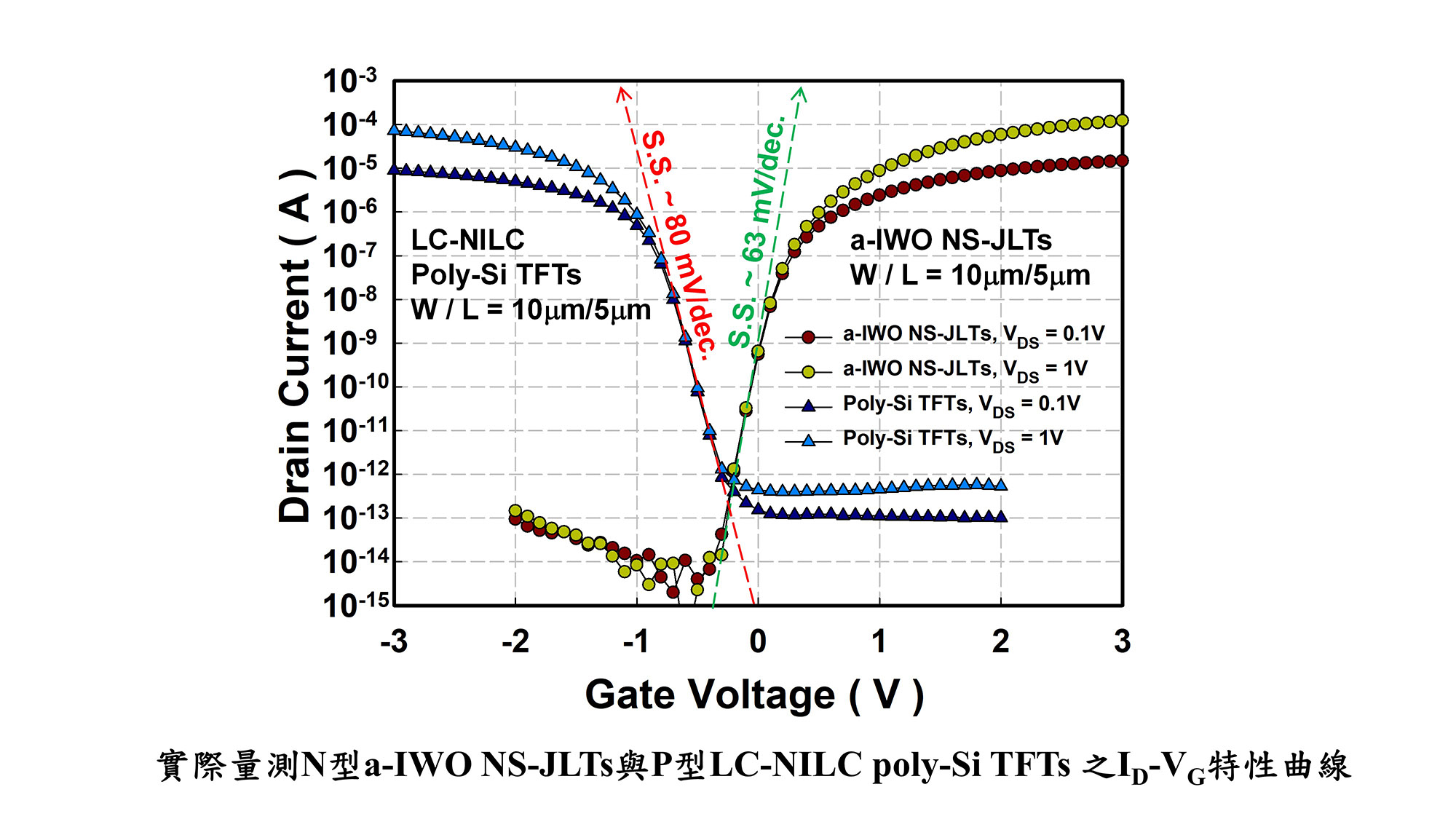
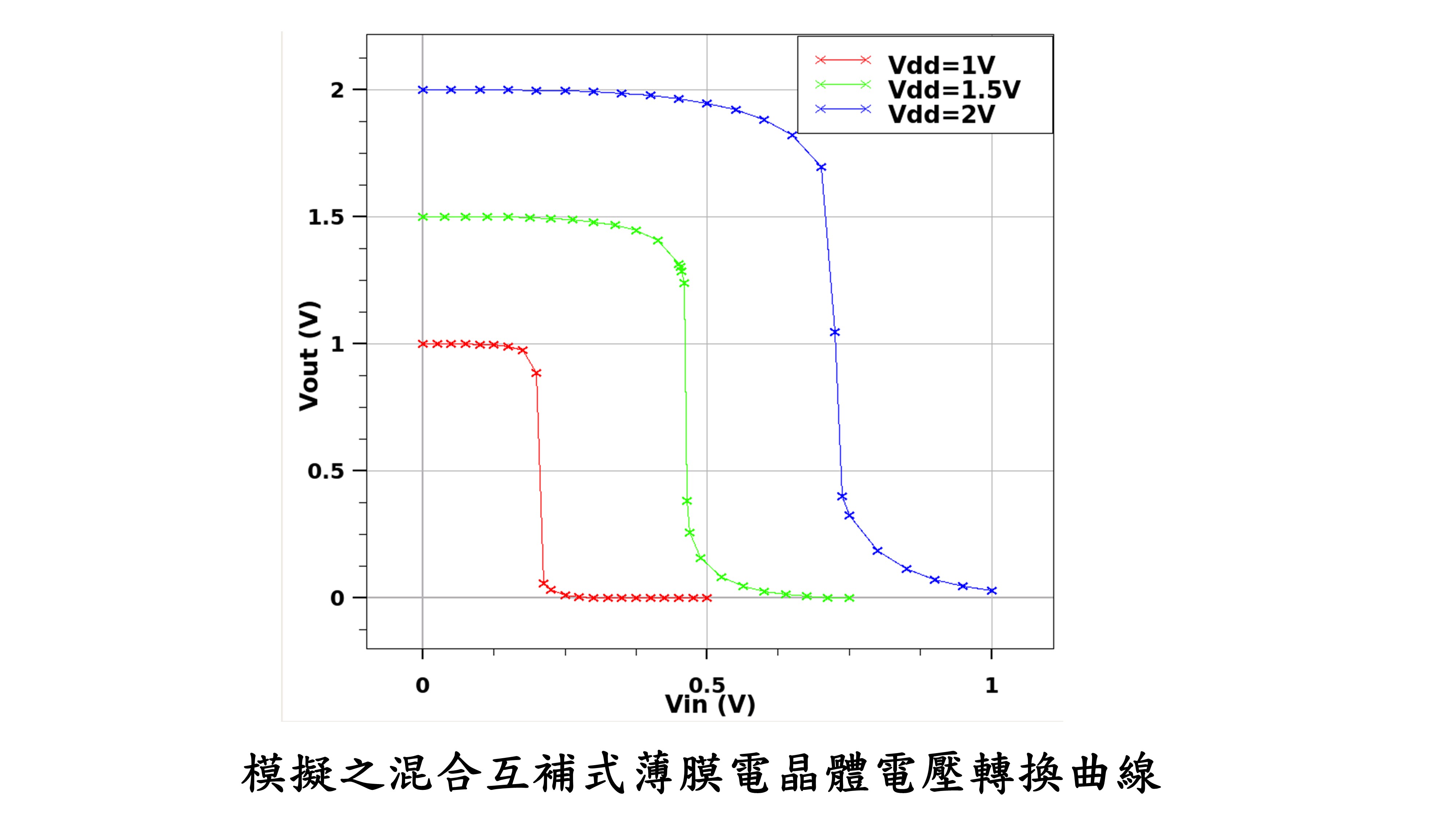
| Scientific Breakthrough | Through silicon via (TSV) technology has been adopted to achieve multi-chip modules with different IC functions for applications in the 3D-IC package architecture. However, the TSV technology suffers many challenges due to the limit in circuit layout and causing the decreased yield. Monolithic 3D-IC technology is expected to replace the TSV due to its ease of manufacture, short interconnections, lower power consumption, and lower cost. In this research, we have successfully developed the high-performance HC-TFTs comprised of N-channel a-IWO nano-sheet TFT and P-channel poly-Si TFT for monolithic 3D CMOS-based inverter applications. The technological breakthroughs are not only applied to 3D-IC, but can also be extended to ultra-high resolution flat-panel display backplane technology. |
||
| Industrial Applicability | This project has successfully developed a 3D-IC-based CMOS inverter circuit with high performance and low power consumption, which can be implemented in advanced electronic products. Also, the novel HC-TFT CMOS technology can be applied to flat-panel displays to construct the complete driving circuits and make the design of display circuits flexible, enhancing the diversity and added values. |
||
| Keyword | Amorphous oxide semiconductor (AOS) Low-temperature polycrystalline silicon (LTPS) Nickel Induced Lateral Crystallization (NILC) Complementary metal-oxide-semiconductor (CMOS) Hybrid complementary TFTs (HC-TFTs) Inverter System-on-Panel (SoP) Technology Computer Aided Design (TCAD) Monolithic 3D-IC | ||
- ptliu@mail.nctu.edu.tw
other people also saw