


| Technical Name | High Performance and High Uniformity p-GaN Gate Power Device on 6-inch SOI substrate Technology Development | ||
|---|---|---|---|
| Project Operator | Chang Gung University | ||
| Project Host | 邱顯欽 | ||
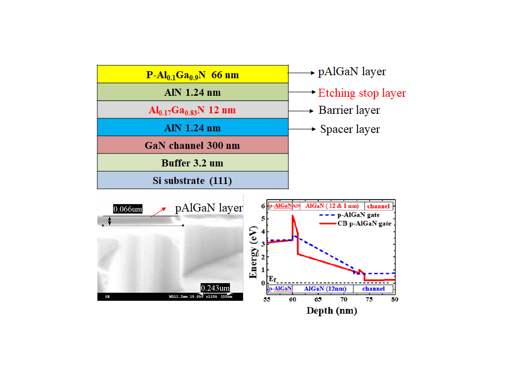
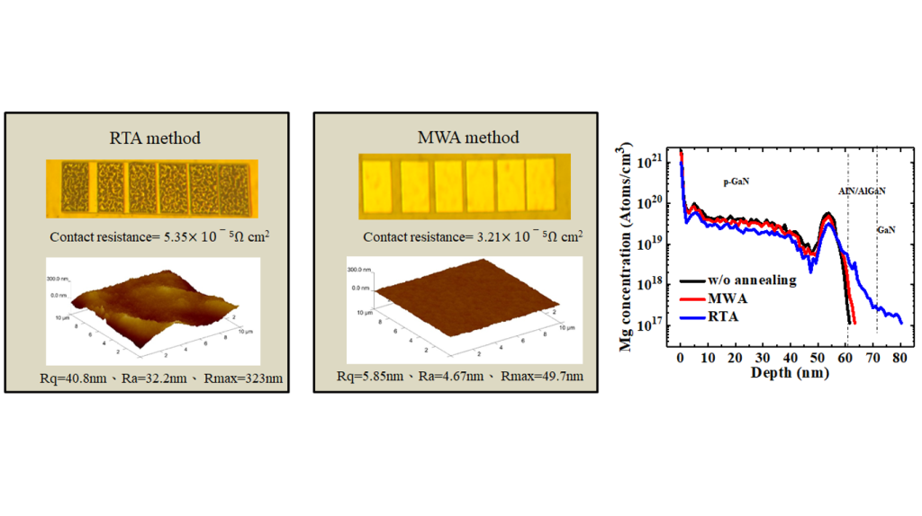
| Summary | We will propose a high device uniformity p-AlGaN gate normally-off power device will be proposed base on AlN etching stop layer design and this composited Schottky barrier layer design can overcome the p-AlGaN over etching problem. Moreover, the microwave annealing technique will also be adopted for this thin composited barrier layer and the Mg out diffusion can also be minimized for p- AlGaN gate. |
||
| Scientific Breakthrough | This major technology breakthrough was described as follows. |
||
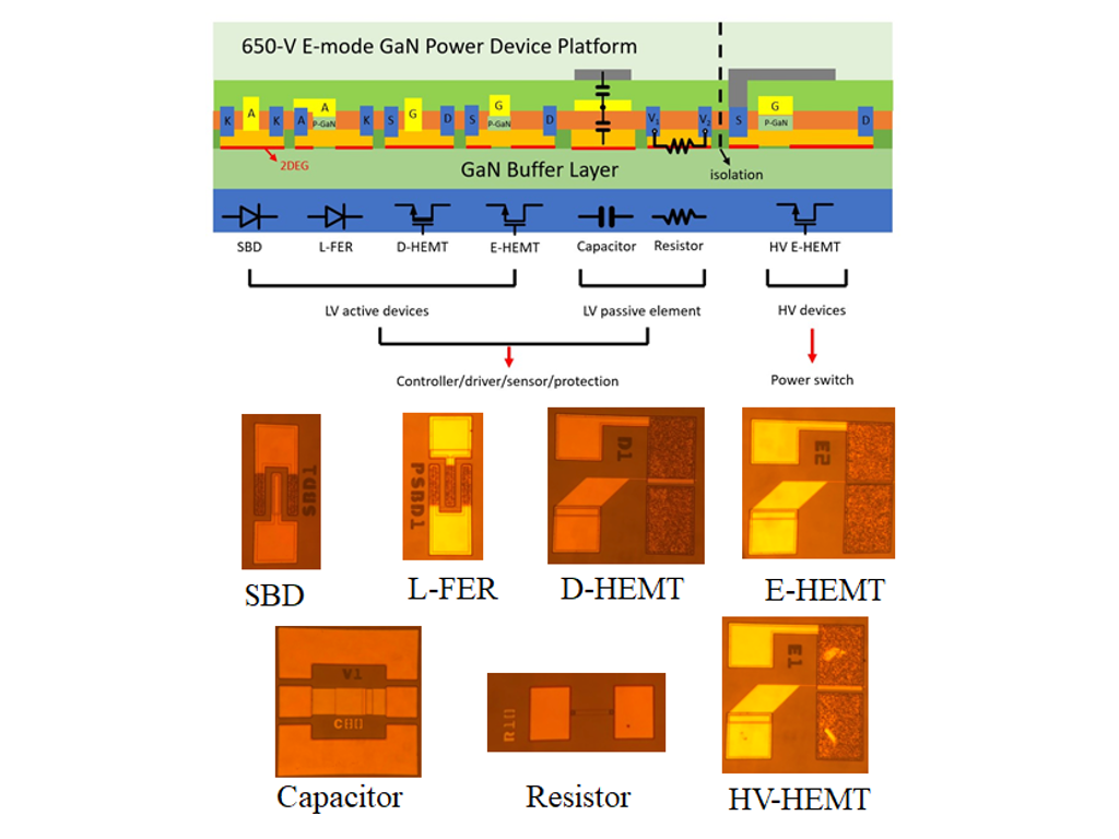
| Industrial Applicability | GaN HEMT devices are used in a wide range of Power design applications including PFC, Power supplies, DC/AC inverter, DC/DC converter, industry inverter, and any Power design application that requires a combination of low power lose and high frequency performance HEMTs. This technology can provide a high device uniformity normally-off GaN power device and high performance. |
||
| Keyword | p-AlGaN Composited Epi Structure Enhance-mode GaN Power device Low turn-on Voltage Power Diode Microwave Annealing Technology SOI Substrate Application High Power AlN Package Compound Semiconductor Logic Circuit Low Damage Etching method Digital Etching Technology | ||
- darrenwang@mail.cgu.edu.tw
other people also saw