


| Technical Name | Epitaxy of Gallium Nitride High Electron Mobility Transistor on Si Substrate | ||
|---|---|---|---|
| Project Operator | National Central University | ||
| Project Host | 綦振瀛 | ||
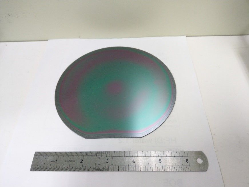
| Summary | The disclosed technology is a metal-organic chemical vapor deposition technology, which enables the epitaxial growth of high quality GaN-based heterostructures on Si substrates. With precise control over the growth parametersepilayer design, AlGaN HEMTs with electron mobility of 2,040 cm2/V-stwo-dimensional electron gas density of 8.8×1012 cm-2 have been demonstrated on 6 inch Si substra |
||
| Scientific Breakthrough | With precise control over the growth parameters, such as growth temperature, reactor pressure, gas flow, type of carrier gas, type of precursor,special design of the epilayer structure, AlGaN, AlInN,AlInGaN HEMTs with excellent electron mobility, low sheet resistance,small wafer bow have been demonstrated on 6 inch Si substrates. |
||
| Industrial Applicability | This technology concerns the epitaxy of GaN-based power transistors on Si substrate for power switchingcommunication applications. Power transistorsRF power amplifiers fabricated on these epitaxial wafers are well suited for high energy efficiency wireless charger, switching power supply, converter, inverter, electrical vehicle, power amplifier for 5G communications,phased array rad |
||
| Keyword | MOCVD AlInN AlGaN GaN on Silicon Epitaxy GaN AlInN High electron mobility transistor AlInGaN RF power amplifier | ||
- s17howard1001@gmail.com
other people also saw