


| Technical Name | MethodStructure of stacking 3D-IC Employing Controlled-Grain Semiconductor Film | ||
|---|---|---|---|
| Project Operator | National Chiao Tung University | ||
| Project Host | 陳冠能 | ||
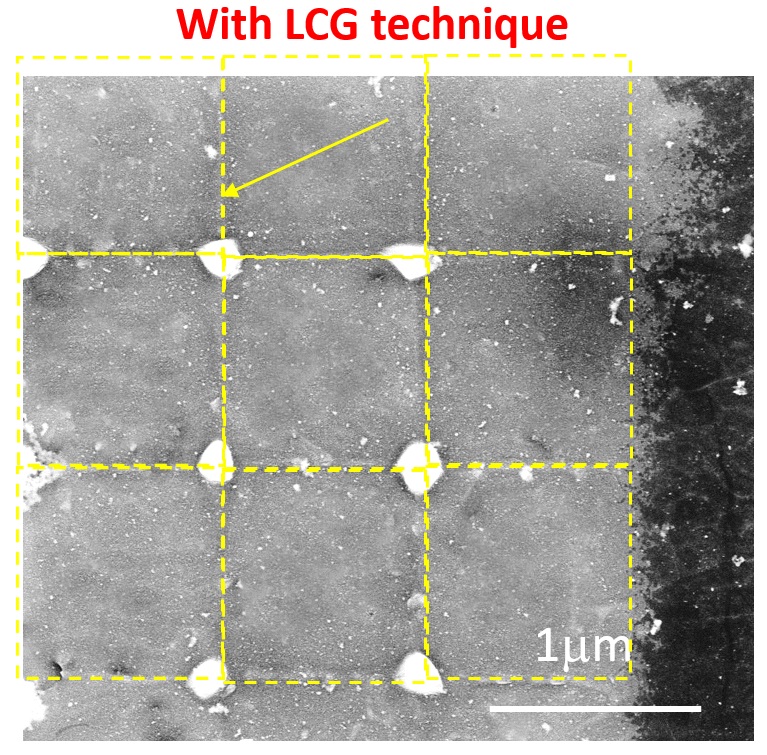
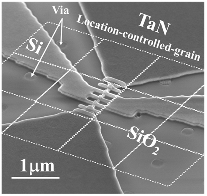
| Summary | The location of controlled-grain Si island is determined by the pattern of “cooling holes”. The grain size is determined by the distance between “holes” due to lateral grain growth using pulse laser crystallization. This predictability allows the transistorscircuits to stay away from the grain boundaries for monolithic |
||
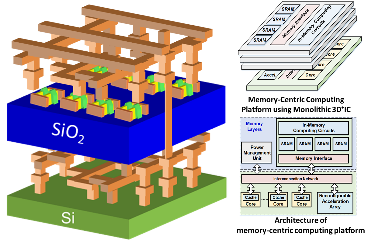
| Scientific Breakthrough | Monolithic 3D integration provides efficient connectivity of circuitsdecrease power consumption, enhance system performancereduce chip size. A BEOL location-controlled technique using pulse laser anneal process for fabricating monolithic 3D FinFET circuits within Si grains is proposed. Spatially separating devicesgrain boundaries provides a promising solution for developing practical monolithic 3D ICs. |
||
| Industrial Applicability | Monolithic 3D integration is an emergingpromising technology that offers a path for high performance, high connectivity, multi-function, smaller form factor,potential cost reduction. It is appropriated for the development of IoT devicesfor the design of neuromorphic computing. |
||
| Keyword | Si thin film location-controlled-grain technique monolithic 3D IC pulsed laser laser annealing FinFET 3D stacking BEOL low temperature process TSV technology | ||
- chia500@yahoo.com.tw
other people also saw